
Thermal Processing of Substrates with Pre- and Post-Spike Temperature Control

a technology of substrates and temperature control, applied in semiconductor devices, laser beam welding apparatus, manufacturing tools, etc., can solve the problems of thermal spike, uncontrollable stress in substrates, and insignificant absorption of doped and undoped silicon, so as to improve the electronic performance of the substrate and reduce stress accumulation

Inactive Publication Date: 2011-12-08
ULTRATECH INT INC
View PDF4 Cites 14 Cited by
  • Summary
  • Abstract
  • Description
  • Claims
  • Application Information

AI Technical Summary

Benefits of technology

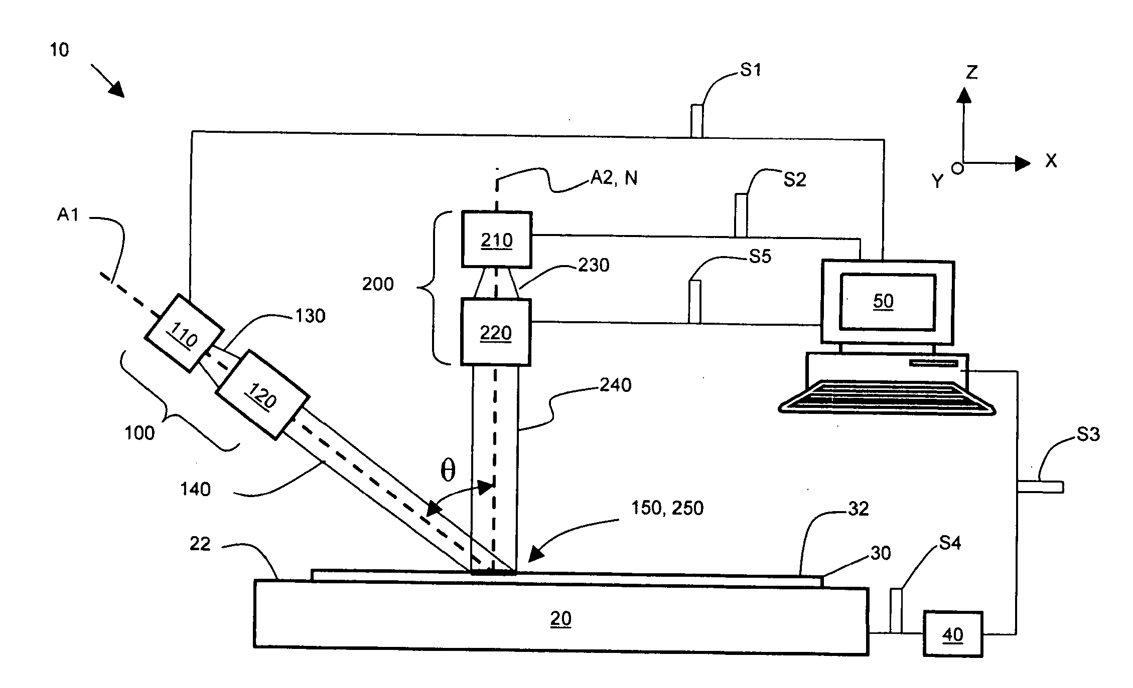
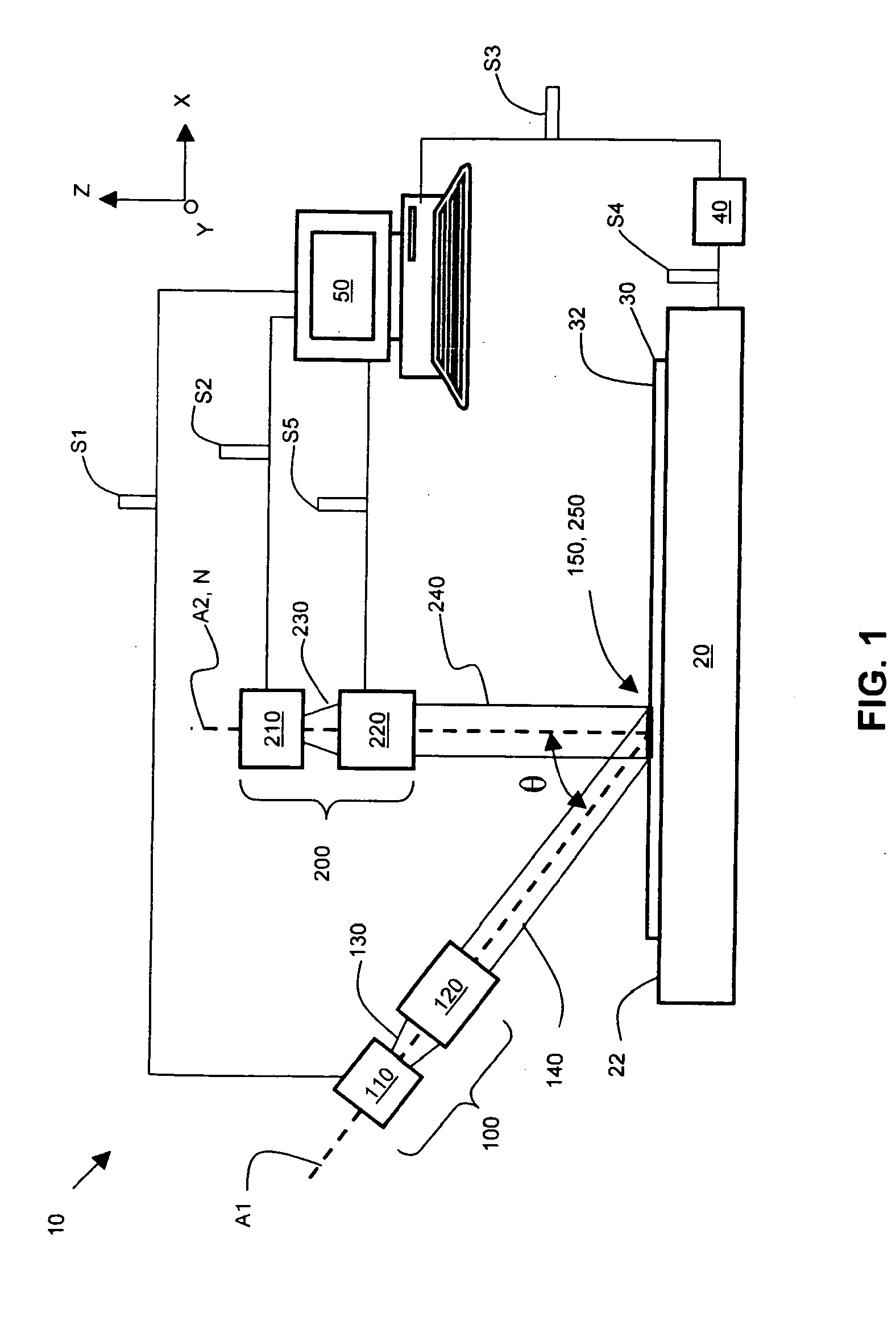
[0012]In an embodiment, the invention provides an apparatus for thermally processing a surface of a substrate. The apparatus include a stage, a plurality of radiation sources, and a controller operatively coupled to the stage and radiation sources. The stage supports the substrate and places the substrate surface in a radiation-receiving position. The radiation sources form images that optionally overlap on the upper substrate surface. The controller provides relative scanning motion between the substrate surface and the images to allow the images to process regions of the substrate surface along a scan path at a substantially uniform peak processing temperature.
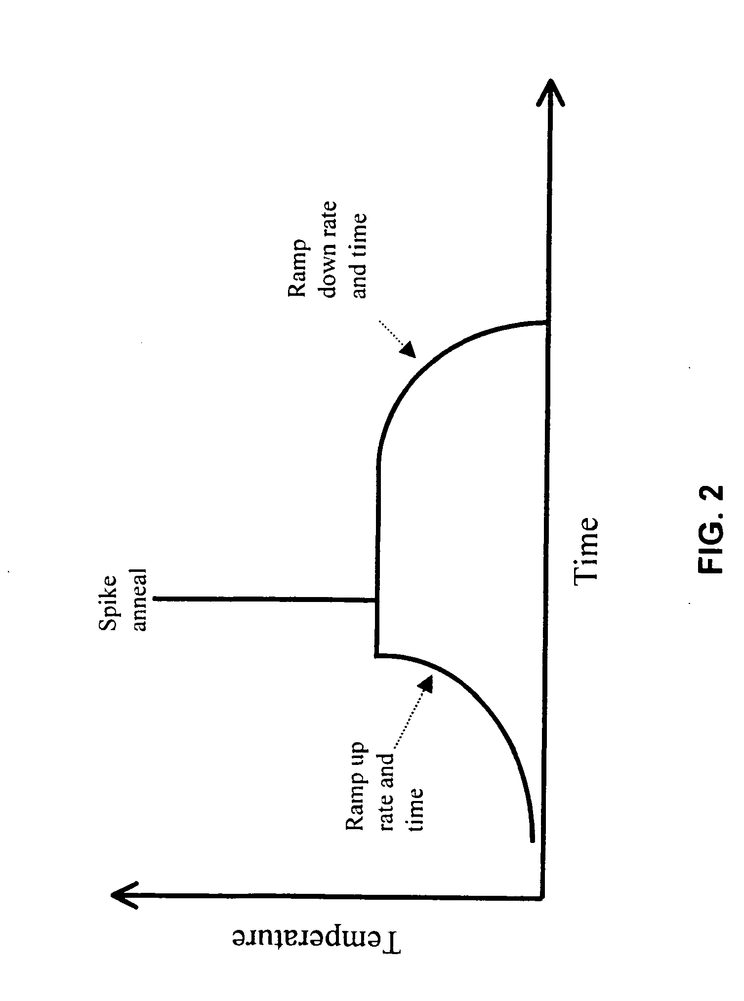
[0014]The heating and / or cooling rates may be selected for a variety of purposes, e.g., to reduce stress accumulation in and / or improve electronic performance of the substrate. In some instances, the prespike heating rate may allow regions of the substrate surface to be heated from the initial temperature to the first intermediate temperature in less than about 2 seconds so the temperature increases in a desired manner to form a desired temperature profile. The temperature profile may be linear or nonlinear. Similarly, the postspike cooling rate may be selected in an analogous manner.

Problems solved by technology

Nevertheless, lightly doped and undoped silicon may not significantly absorb radiation from a CO2 laser spike annealing beam of 10.6 pm radiation at temperatures significantly below about 400° C. because beam's photon energy is less than the bandgap energy of undoped silicon.
Typically, a peak temperature is reached in a short amount of time, thereby resulting in a thermal spike.
Nevertheless, uncontrolled heating and / or cooling may introduce uncontrolled stresses in substrates.
In extreme cases, uncontrolled stresses may result in catastrophic mechanical failure leading to substrate breakage.
Also, simple laser annealing with a single dwell time may not provide optimal electronic performance for the devices.

Method used


Image

  • Thermal Processing of Substrates with Pre- and Post-Spike Temperature Control
  • Thermal Processing of Substrates with Pre- and Post-Spike Temperature Control
  • Thermal Processing of Substrates with Pre- and Post-Spike Temperature Control

Examples


Embodiment Construction

Definitions and Overview

[0029]Before describing the present invention in detail, it is to be understood that this invention, unless otherwise noted, is not limited to specific substrate constructions, substrate materials, radiation sources, as such may vary. It is also to be understood that the terminology used herein is for the purpose of describing particular embodiments only, and is not intended to be limiting.

[0030]It must be noted that, as used in this specification and the appended claims, the singular forms “a”, “an” and “the” include both singular and plural referents unless the context clearly dictates otherwise. Thus, for example, reference to “beam” includes a plurality of beams as well as a single beam, reference to “a wavelength” includes a range or plurality of wavelengths as well as a single wavelength, reference to “a region” includes a combination of regions as well as single region, and the like.

[0031]In describing and claiming the present invention, the following ...


PUM

PropertyMeasurementUnit
dwell timeaaaaaaaaaa
temperatureaaaaaaaaaa
temperaturesaaaaaaaaaa

Abstract

Provided are apparatuses and method for the thermal processing of a substrate surface, e.g., controlled laser thermal annealing (LTA) of substrates. The invention typically involves irradiating the substrate surface with first and second images to process regions of the substrate surface at a substantially uniform peak processing temperature along a scan path. A first image may serve to effect spike annealing of the substrates while another may be used to provide auxiliary heat treatment to the substrates before and / or after the spike annealing. Control over the temperature profile of the prespike and / or postspike may also reduce stresses and strains generated in the wafers. Also provided are microelectronic devices formed using the inventive apparatuses and methods.

Description

BACKGROUND OF THE INVENTION[0001]1. Field of the Invention[0002]The present invention relates to thermal processing of substrates using a plurality of radiation sources that generate first and second images that optionally overlap. In particular, the invention relates to such processing wherein regions of the substrate surface are each processed at an optionally controlled prespike temperature, followed by a controlled uniform peak temperature, followed by an optionally controlled postspike temperature.[0003]2. Description of Related Art[0004]Fabrication of semiconductor-based microelectronic devices often involves subjecting a semiconductor substrate “thermal processing” to activate dopant atoms implanted in junction regions (e.g., source and drain regions) of the substrate. For example, the source / drain parts of transistors may be formed by exposing regions of a silicon wafer to electrostatically accelerated dopants. After implantation, the dopants are electrically inactive. Activ...

Claims


Application Information

Patent Timeline
Patent Type & Authority Applications(United States)
IPC IPC(8): H01L21/324H01L29/02
CPCB23K26/0608B23K26/073H01L21/268B23K26/083B23K26/0807B23K26/082H01L21/02H01L21/324
Inventor ZAFIROPOULO, ARTHUR W.HAWRYLUK, ANDREW M.MCWHIRTER, JAMES T.ANIKITCHEV, SERGUEI G.
Owner ULTRATECH INT INC
Learn More