Group iib/va semiconductors suitable for use in photovoltaic devices

a photovoltaic device and semiconductor technology, applied in semiconductor/solid-state device manufacturing, semiconductor devices, electrical equipment, etc., can solve the problems of poor photovoltaic behavior of devices, poor film quality, and difficult preparation of n-type zinc phosphide, and achieve the effect of improving the electronic performance of semiconductor materials

Inactive Publication Date: 2011-12-22
CALIFORNIA INST OF TECH +1
View PDF1 Cites 17 Cited by
  • Summary
  • Abstract
  • Description
  • Claims
  • Application Information

AI Technical Summary

Benefits of technology

[0008]The present invention relates to devices, particularly photovoltaic devices, incorporating Group IIB / VA semiconductors such as phosphides, arsenides, and / or antimonides (also collectively referred to in the art as pnictides) of one or more of Zn and / or Cd. In particular, the present invention relates to methodologies, resultant products, and precursors thereof in which electronic performance of the semiconductor material is improved by causing the Group IIB / VA semiconductor material to react with at least one metal-containing species (hereinafter co-reactive species) that is sufficiently co-reactive with at least one Group VA species incorporated into the Group IIB / VA semiconductor as a lattice substituent (recognizing that the same and / or another Group VA species also optionally may be incorporated into the Group IIB / VA semiconductor in other ways, e.g., as a dopant or the like).
[0009]In some embodiments, the reaction may occur by heating the semiconductor material while in contact with the co-reactive species, although heating may not be required when the co-reactive species is sufficiently reactive. In representative embodiments, it is believed that the reaction may form p / n homojunction, heterojunction, and / or passivating features with improved resolution and quality.
[0012]The reaction also is believed to provide a passivation effect in which the interface between the Group IIB / VA semiconductor material and overlying layers is improved. Without wishing to be bound, it is believed that the reaction between Group VA material of the semiconductor and the co-reactive species helps to provide a transition region in situ whose formation helps to remove defects and native oxide to provide the passivation. As one example, the reaction between Ca and zinc phosphide could yield a passivating region including calcium phosphide proximal to the original interface between the zinc phosphide and the calcium in the article being treated.

Problems solved by technology

Preparing n-type zinc phosphide, particularly using methodologies suitable for the industrial scale, remains challenging.
However, such approaches generally yield devices with poor photovoltaic behavior, if any, due at least in part to poor film quality, lack of control over film stoichiometry, and / or lack of control over formation of high quality p / n junctions.

Method used


Image

  • Group iib/va semiconductors suitable for use in photovoltaic devices
  • Group iib/va semiconductors suitable for use in photovoltaic devices
  • Group iib/va semiconductors suitable for use in photovoltaic devices

Examples


example 1

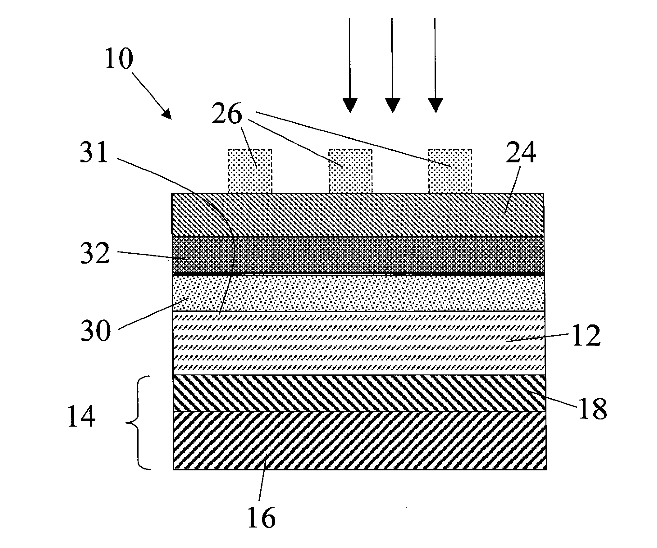
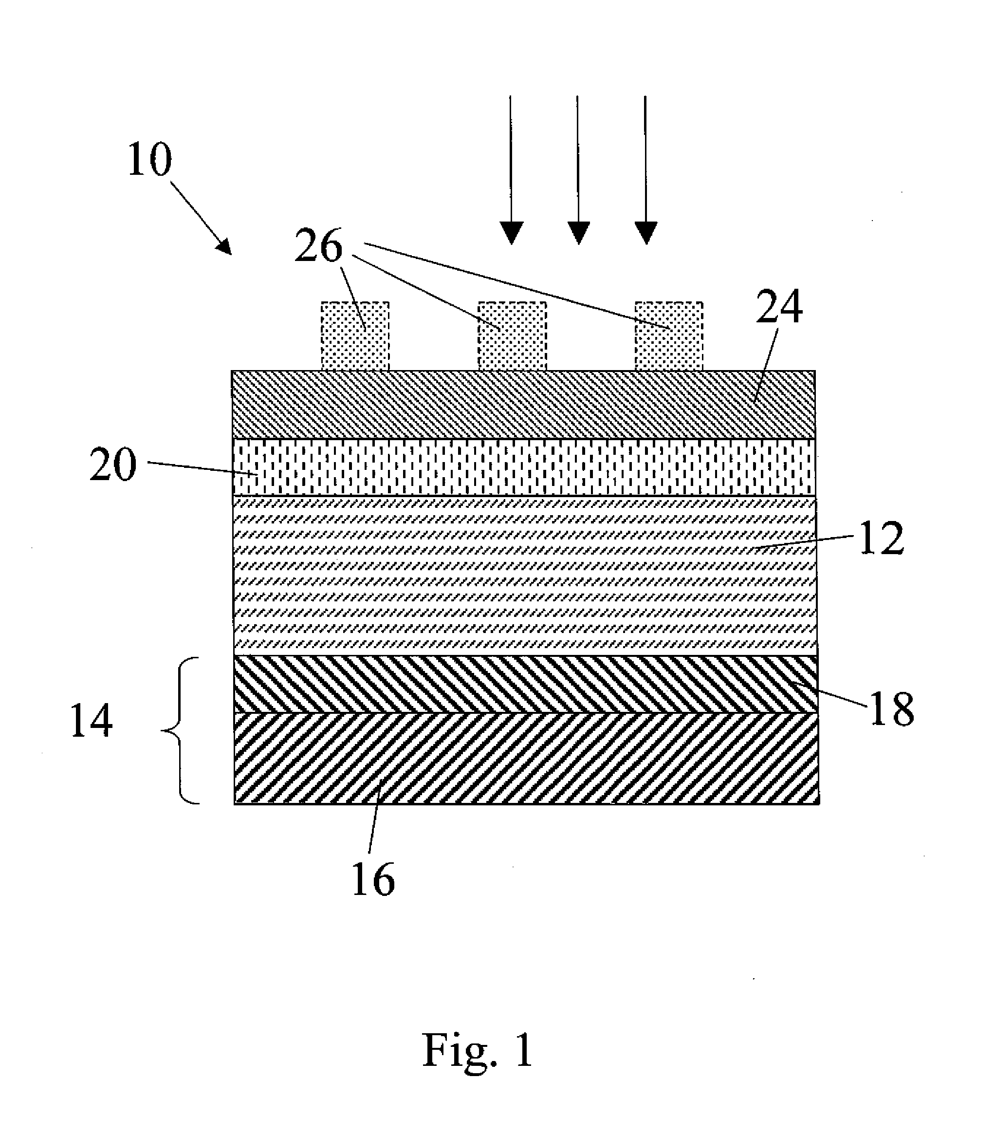
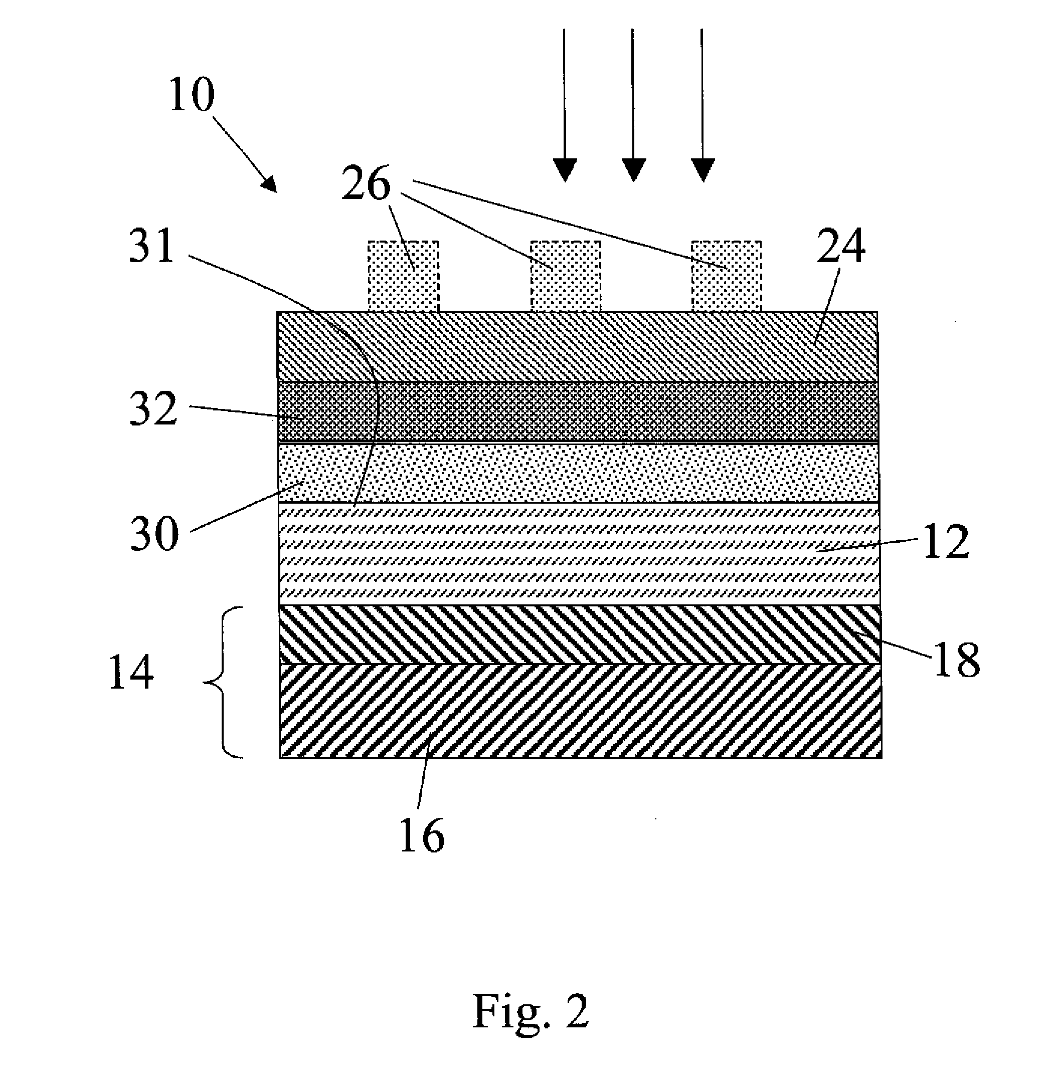
[0102]The Zn3P2 samples used in this example are grown by a physical vapor transport process. Red phosphorus chips and zinc shot (99.9999%) are combined at 850° C. to form Zn3P2 powders. The powders are then processed using crystal growth techniques into polycrystalline boules 1 cm in diameter and 4 cm in length, with grain sizes of ˜1-5 mm2. The resulting crystals are diced with a diamond saw and have as-grown resistivity between 100-2000 Ωcm. Annealing with white phosphorus in sealed ampoules at 400° C. for 20 hours is effective at reducing the wafer resistivity to ˜20 Ωcm due to doping by phosphorus interstitials. Both undoped and P-doped samples are polished with diamond paste to produce Zn3P2 wafers. Samples with 1 cm diameter and 500-600 μm thickness are etched for 30 s in 2-3% (v:v) Br2 in CH3OH, rinsed in CH3OH, dried under a stream of N2, and used promptly thereafter.

[0103]ITO / Ca / Zn3P2 solar cells are fabricated from P-doped Zn3P2 samples. Freshly etched wafers are patterne...

example 2

[0104]As a way of testing the reactivity of Ca as well as another co-reactive metal other than Ca, a set of devices composed of an ITO capping layer (100 nm), a co-reactive metal (50 nm), an etched and polished Zn3P2 substrate, and a Ag back contact (200 nm) were fabricated. In one set of devices, Ca was used as the co-reactive metal. In another set of devices, Mg was used as the co-reactive metal. Typically the Voc of photolithographically-defined devices using >99% Mg as the co-reactive metal are low, oc due to the reaction between the co-reactive metal and Zn3P2. Devices incorporating Ca metal as the co-reactive species show significantly higher Voc as-fabricated. The observation of Voc>380 mV in as-fabricated devices utilizing Ca is consistent with the expected higher reactivity of Ca metal with the phosphorus in Zn3P2 as compared to Mg when used as a co-reactive species (as distinguished from the use of Mg as a capping layer as described further below). The devices were charact...

example 3

[0106]Solar cells are made in accordance with Example 1 except that for each cell in this example, Sr or Ti, respectively, is substituted for Ca.


PUM

PropertyMeasurementUnit
band gapaaaaaaaaaa
open circuit voltageaaaaaaaaaa
thicknessaaaaaaaaaa

Abstract

The present invention relates to devices, particularly photovoltaic devices, incorporating Group IIB / VA semiconductors such phosphides, arsenides, and / or antimonides of one or more of Zn and / or Cd. In particular, the present invention relates to methodologies, resultant products, and precursors thereof in which electronic performance of the semiconductor material is improved by causing the Group IIB / VA semiconductor material to react with at least one metal-containing species (hereinafter co-reactive species) that is sufficiently co-reactive with at least one Group VA species incorporated into the Group IIB / VA semiconductor as a lattice substituent (recognizing that the same and / or another Group VA species also optionally may be incorporated into the Group IIB / VA semiconductor in other ways, e.g., as a dopant or the like).

Description

PRIORITY[0001]The present nonprovisional patent Application claims priority under 35 U.S.C. §119(e) from U.S. Provisional patent application having Ser. No. 61 / 355,344, filed on Jun. 16, 2010, by Kimball et al. and titled IMPROVED GROUP IIB / VA SEMICONDUCTORS SUITABLE FOR USE IN PHOTOVOLTAIC DEVICES, wherein the entirety of said provisional patent application is incorporated herein by reference.FIELD OF THE INVENTION[0002]The present invention relates to photovoltaic devices incorporating Group IIB / VA semiconductors such as phosphides, arsenides, and / or antimonides of one or more of Zn and / or Cd. In particular, the present invention relates to methodologies, resultant products, and precursors thereof in which electronic performance of the semiconductor material is improved by heating the semiconductor material while in contact with at least one material (e.g. Mg, Ca, Sr, Ba, Sc, Y, Ti, Zr, V, Cr, Nb, Mo, Hf and / or the like) that is co-reactive with a Group VA element.BACKGROUND OF TH...

Claims


Application Information

Patent Timeline
Patent Type & Authority Applications(United States)
IPC IPC(8): H01L31/18H01L29/24
CPCH01L31/032H01L31/0321Y02E10/547H01L31/18H01L31/068
Inventor KIMBALL, GREGORY M.DEGROOT, MARTY W.LEWIS, NATHAN S.ATWATER, HARRY A.
Owner CALIFORNIA INST OF TECH
Why Eureka
Try Eureka