Semiconductor device and the method of manufacturing the same

a semiconductor and semiconductor technology, applied in the direction of semiconductor devices, basic electric elements, electrical equipment, etc., can solve the problems of increasing the manufacturing cost of the wafer, and affecting the electric characteristics of the vertical-field plate-type mosfet, so as to facilitate the reduction of only the impurity concentration and reduce the on-state resistance. , the effect of reducing the impurity concentration

Active Publication Date: 2011-12-15
FUJI ELECTRIC CO LTD
View PDF0 Cites 56 Cited by
  • Summary
  • Abstract
  • Description
  • Claims
  • Application Information

AI Technical Summary

Benefits of technology

[0067]By arranging the fourth semiconductor region, only the impurity concentration in the portion of the first semiconductor region in the vicinity of the trench bottom surface is set to be low. By the impurity concentration setting, the impurity concentration in the region that will work as a channel region is set to be higher than the impurity concentration in the vicinity of the trench bottom surface. Therefore, the ON-state resistance is reduced. By lowering the impurity concentration in the vicinity of the trench bottom surface, the electric field in the vicinity of the trench bottom surface is relaxed.
[0068]Since the fourth semiconductor region facilitates lowering only the impurity concentration in the vicinity of the trench bottom surface, it is not necessary to provide the first semiconductor region with a double-layer epitaxial structure. Therefore, the portion of the first semiconductor region, in which the impurity concentration is low, is made to be narrower as compared with the case, in which the first semiconductor region is provide with a double-layer epitaxial structure. Due to this, the impurity concentration in the entire first semiconductor region is made to be higher than the impurity concentration in the entire drift region of the conventional semiconductor device which employs a double-layer epitaxial structure. Therefore, the ON-state resistance is reduced and the electric field in the vicinity of the trench bottom surface is relaxed more effectively as compared with the conventional vertical-field-plate-type semiconductor device (cf. FIG. 16).
[0069]Since it is not necessary to provide the first semiconductor region with a double-layer epitaxial structure, the conventional edge-termination structure is employable. Therefore, the manufacturing costs of a wafer, in which the semiconductor device is formed, are reduced.
[0070]According to the subject matter of the appended claim 4, the arrangement of the fifth semiconductor region facilitates setting the impurity concentration to be high in the portion of the first semiconductor region that will work as a channel region. The arrangement of the fifth semiconductor region facilitates increasing the carrier amount injected from the second semiconductor region to the first semiconductor region. Therefore, the ON-state resistance is reduced.

Problems solved by technology

However, the techniques described above increase the manufacturing costs of the wafer, in which a vertical-field-plate-type MOSFET is formed.
In addition, crystal defects increase in the drift region and the electric characteristics of the vertical-field-plate-type MOSFET are impaired.

Method used


Image

  • Semiconductor device and the method of manufacturing the same
  • Semiconductor device and the method of manufacturing the same
  • Semiconductor device and the method of manufacturing the same

Examples


first embodiment

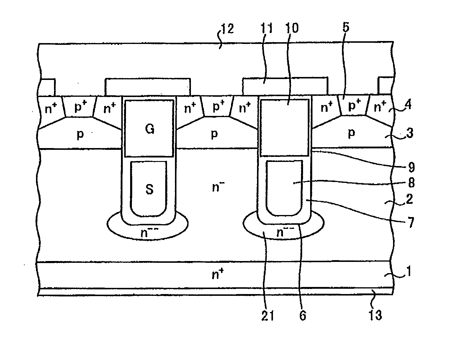
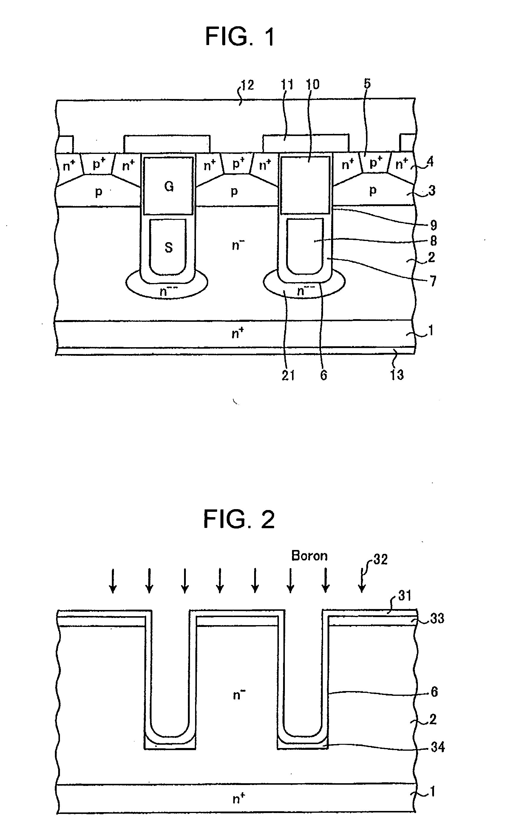
[0099]FIG. 1 is the cross sectional view of a semiconductor device according to a first embodiment of the invention.

[0100]The semiconductor device shown in FIG. 1 is a MOSFET having a vertical field-plate structure (hereinafter referred to as a “vertical-field-plate-type MOSFET”). The vertical field-plate structure includes field plate (first electrode) 8 biased at a source potential and gate electrode (control electrode) 10, both buried in trench 6 formed in a semiconductor substrate. The semiconductor substrate includes n+ drain region 1 and n− drift region (first semiconductor region) 2 on n+ drain region 1. The semiconductor substrate may be a silicon (Si) substrate or a silicon carbide (SiC) substrate.

[0101]In detail, an active area, in which a vertical-field-plate-type MOSFET is formed, and an edge-termination area (not shown) surrounding the active area are arranged in n− drift region 2. The edge-termination area functions to improve the breakdown voltage of the active area. ...

second embodiment

[0123]FIG. 8 is the cross sectional view of a semiconductor device according to a second embodiment of the invention.

[0124]The n−− lightly doped region may be arranged only in the corner portion of trench 6 in the semiconductor device according to the first embodiment.

[0125]According to the second embodiment, lightly doped region (fourth semiconductor region) 22 covers only the corner portion of trench 6 as shown in FIG. 8. In other words, the impurity concentration of n− lightly doped region 2 in the corner portion of trench 6 is reduced. Due to the impurity concentration setting, a depletion layer is made to expand easily, in the same manner as according to the first embodiment, in the vicinity of the trench 6 corner portion, to which the electric field is liable to localize. Therefore, the electric field in the vicinity of the trench 6 corner portion is relaxed and the breakdown voltage in the active area is prevented from lowering. The other structures are the same with those ac...

third embodiment

[0136]FIG. 12 is the cross sectional view of a semiconductor device according to a third embodiment of the invention. An n-type heavily doped region may be disposed in n− drift region 2 instead of the n−− lightly doped region covering the trench bottom surface in the semiconductor device according to the first embodiment.

[0137]As shown in FIG. 12, n-type heavily doped region (fifth semiconductor region) 23 is formed on the p-type well region 3 side of the trench 6 corner portion in n− drift region 2. The impurity concentration in n-type heavily doped region 23 is higher than the impurity concentration in n− drift region 2. It is preferable for the impurity concentration in n-type heavily doped region 23 to be between 114% and 500% of the impurity concentration in n− drift region 2. It is effective for n-type heavily doped region 23 to be adjoining to field plate 8 and gate electrode 10 via first insulator film 7 and second insulator film 9 formed on the trench 6 side wall.

[0138]By d...


PUM


Abstract

A semiconductor device according to the invention includes p-type well region 3 and n+ source region 4, both formed selectively in the surface portion of n drift region 2; trench 6 in contact with n+ source region 4 and extending through p-type well region 3 into n drift region 2; field plate 8 formed in trench 6 with first insulator film 7 interposed between the trench 6 inner surface and field plate 8; gate electrode 10 formed in trench 6 with second insulator film 9 interposed between the trench 6 side wall and gate electrode 10, gate electrode 10 being formed above field plate 8; first insulator film 7 being thicker than second insulator film 9; and n−− lightly doped region 21 in n drift region 2, n−− lightly doped region 21 crossing under the bottom surface of trench 6 from the corner portion thereof, n−− lightly doped region 21 covering the bottom surface of trench 6.
The semiconductor device according to the invention and the method of manufacturing the semiconductor device according to the invention facilitate lowering the ON-state voltage, preventing the breakdown voltage from lowering, lowering the gate capacitance, and reducing the manufacturing costs.

Description

FIELD OF THE INVENTION[0001]The present invention relates to semiconductor devices and the method of manufacturing the semiconductor devices.BACKGROUND[0002]As one of the metal-oxide-semiconductor field-effect transistors (hereinafter referred to as the “MOSFET's”) having a trench-structure, a MOSFET having a field-plate structure including a field plate biased at a source potential and formed in the bottom of a trench, in which a gate electrode is formed, is known to the persons skilled in the art. Hereinafter, the field-plate structure described above will be referred to as a “vertical field-plate structure”. By providing a MOSFET with the vertical field-plate structure, the breakdown voltage will be lowered hardly, even if the impurity concentration in the drift region is high. Therefore, the ON-state voltage is reduced and the gate capacitance (parasitic capacitance) is reduced.[0003]FIG. 16 is the cross sectional view of a conventional MOSFET having a vertical field-plate struc...

Claims


Application Information

Patent Timeline
Patent Type & Authority Applications(United States)
IPC IPC(8): H01L29/78H01L21/265
CPCH01L21/26586H01L29/0878H01L29/407H01L29/7827H01L29/66734H01L29/7813H01L29/66666H01L29/42368H01L29/401H01L21/2253H01L29/1608H01L29/66068
Inventor NISHIMURA, TAKEYOSHI
Owner FUJI ELECTRIC CO LTD
Why Eureka
Try Eureka