Method For Producing Semiconductor Wafers Composed Of Silicon

Active Publication Date: 2011-12-15
SILTRONIC AG
View PDF4 Cites 11 Cited by
  • Summary
  • Abstract
  • Description
  • Claims
  • Application Information

AI Technical Summary

Benefits of technology

[0009]It is an object of the present invention to propose a method which comprises at least one measure which counteracts the formation of pinhole defects in the single crystal and which is effective during the process of pulling the single crystal. These and other objects are achieved by means of a method for producing semiconductor wafers composed of silicon, comprising p

Problems solved by technology

Semiconductor wafers in which such pinhole defects are present are unusable as substrate wafers for producing electronic components.
However, the crucibles improved in this respect generally are more expensive or entail other disadvantages, for example because they liberate substance

Method used


Image

  • Method For Producing Semiconductor Wafers Composed Of Silicon
  • Method For Producing Semiconductor Wafers Composed Of Silicon
  • Method For Producing Semiconductor Wafers Composed Of Silicon

Examples


example

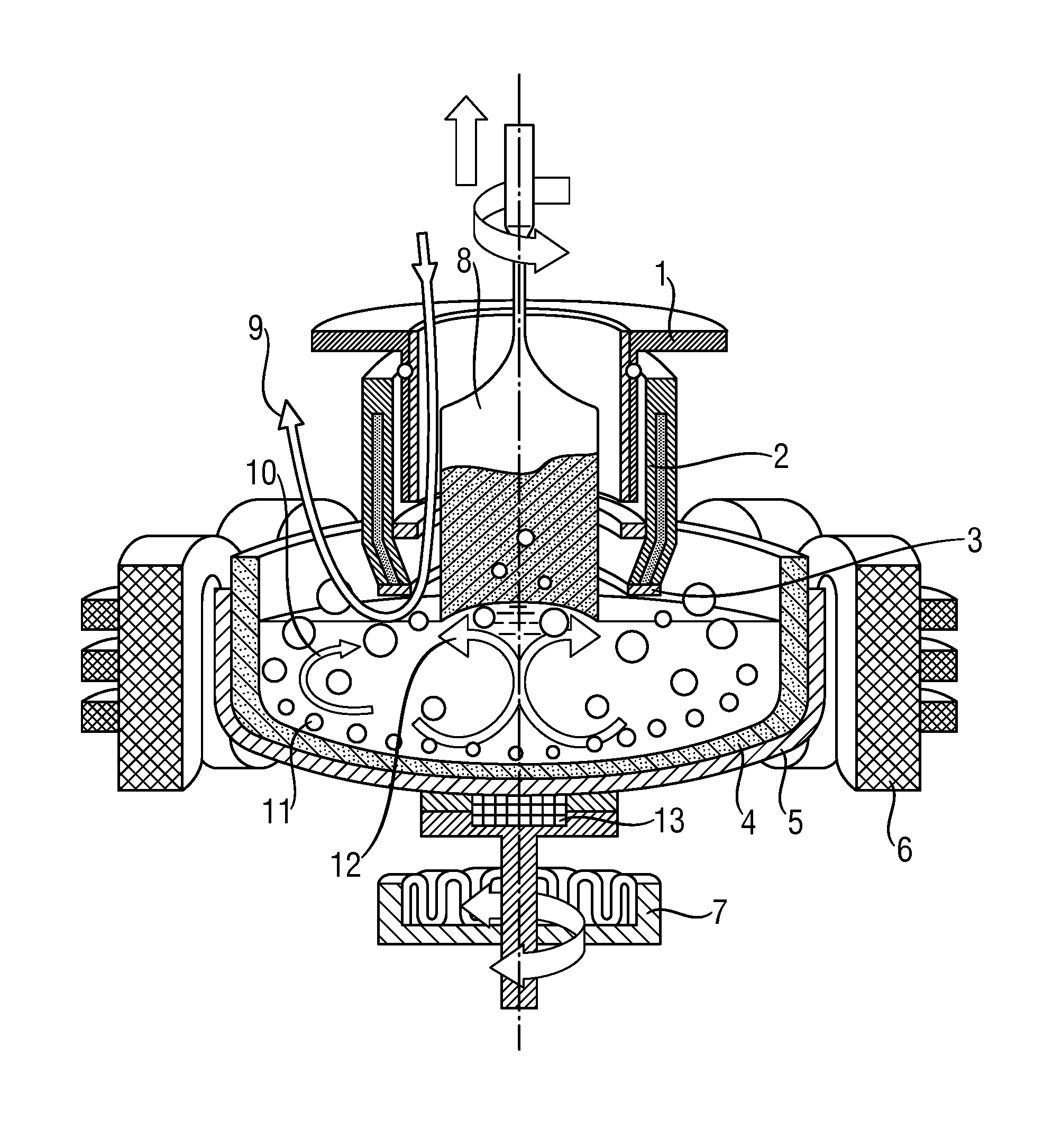
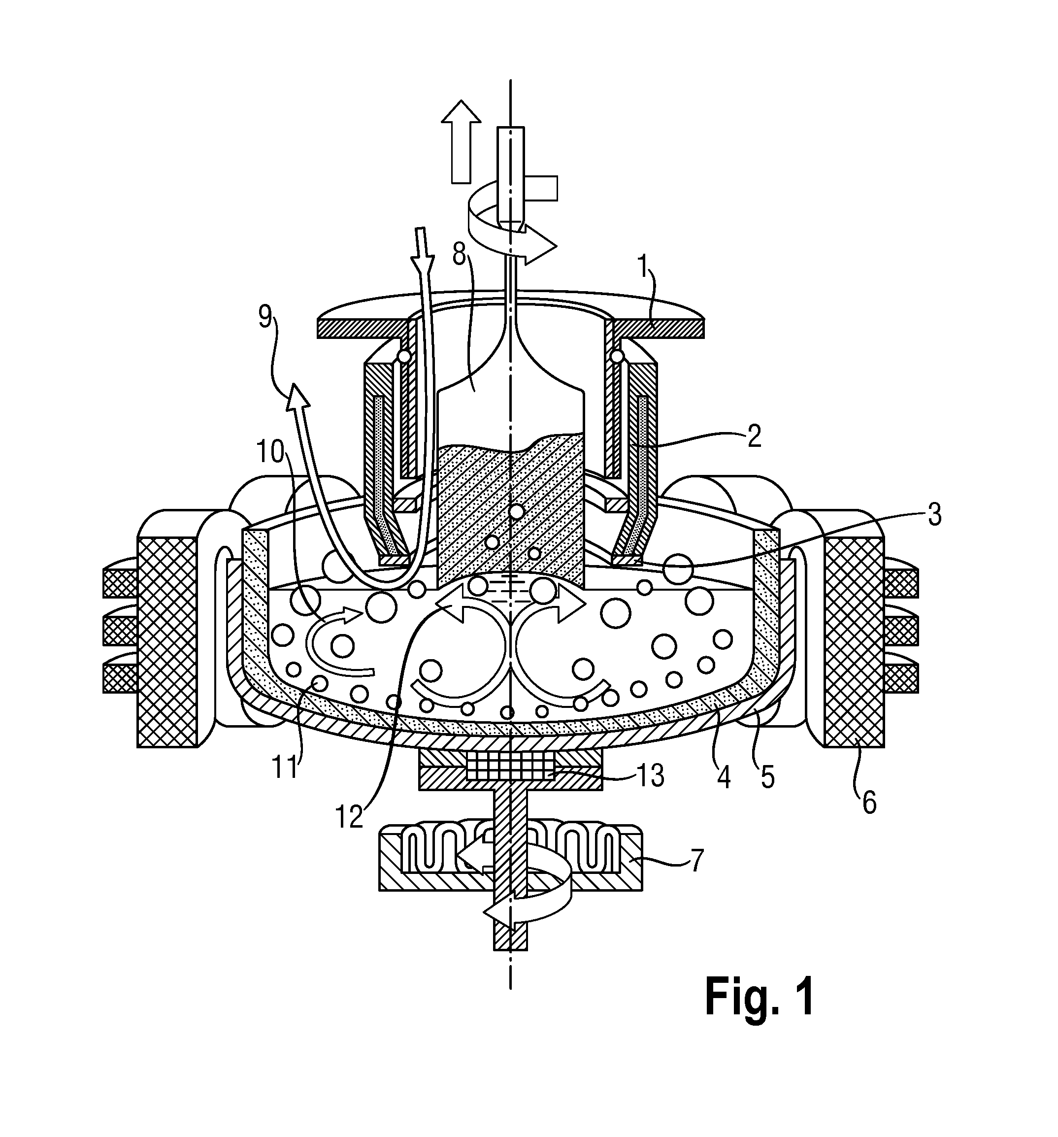
[0027]A series of single crystals composed of silicon having a nominal diameter of 300 mm were pulled from a crucible having a diameter of 28 inches (711.2 mm) by means of the arrangement shown in FIG. 1, in accordance with the method according to the invention. The average crystal lifting speed was 0.55 mm / min during the process of pulling the cylindrical section of a single crystal. At the beginning of the process of pulling the cylindrical section of a single crystal, the heating power of the crucible bottom heater was altered once in accordance with the ramp illustrated in FIG. 3. For comparison purposes, further single crystals were pulled under the same conditions, but without this alteration of the heating power of the crucible bottom heater. A statistical evaluation of the frequency of the occurrence of pinhole defects revealed a failure frequency approximately 30 times higher, on average, on account of such defects in the case of the semiconductor wafers that had been slice...


PUM

PropertyMeasurementUnit
Lengthaaaaaaaaaa
Timeaaaaaaaaaa
Timeaaaaaaaaaa

Abstract

Silicon semiconductor wafers are produced by pulling a single crystal at a seed crystal from a melt heated in a crucible; supplying heat to the center of the crucible bottom with a heating power which, in the course of the growth of a cylindrical section of the single crystal, is increased at least once to not less than 2 kW and is then decreased again; and slicing semiconductor wafers from the pulled single crystal.

Description

CROSS-REFERENCE TO RELATED APPLICATIONS[0001]This application claims priority to German Patent Application No. DE 102010023101.0 filed Jun. 9, 2010 which is herein incorporated by reference.BACKGROUND OF THE INVENTION[0002]1. Field of the Invention[0003]The invention relates to a method for producing semiconductor wafers composed of silicon, comprising pulling a single crystal at a seed crystal from a melt heated in a crucible, supplying heat to the center of the crucible bottom, and slicing the semiconductor wafers from the pulled single crystal.[0004]2. Background Art[0005]The crucible used for Czochralski silicon single crystal growth usually consists of a material containing silicon dioxide, such as quartz. It is generally filled with chunks and / or with granules composed of polycrystalline silicon, the latter being melted with the aid of a side heater arranged around the crucible. After a phase of thermal stabilization of the melt, a monocrystalline seed crystal is dipped into t...

Claims


Application Information

Patent Timeline
IPC IPC(8): B28B11/14
CPCC30B15/18C30B29/06C30B15/305C30B15/20H01L21/02B28D5/00
Inventor WEBER, MARTINSCHACHINGER, WERNERFILAR, PIOTR
Owner SILTRONIC AG
Why Eureka
Try Eureka