Switching power source apparatus
- Summary
- Abstract
- Description
- Claims
- Application Information
AI Technical Summary
Benefits of technology
Problems solved by technology
Method used
Image
Examples
embodiment 1
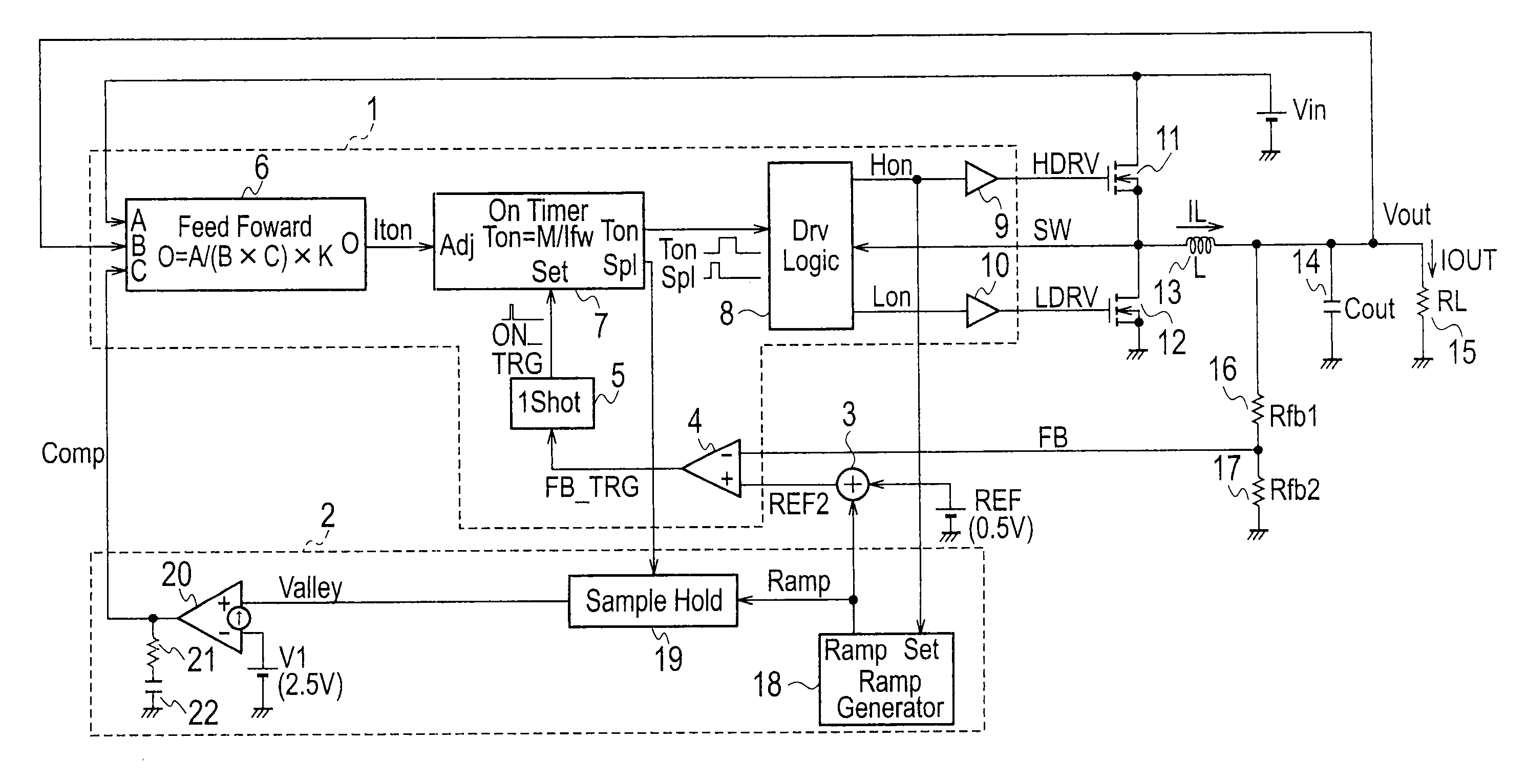
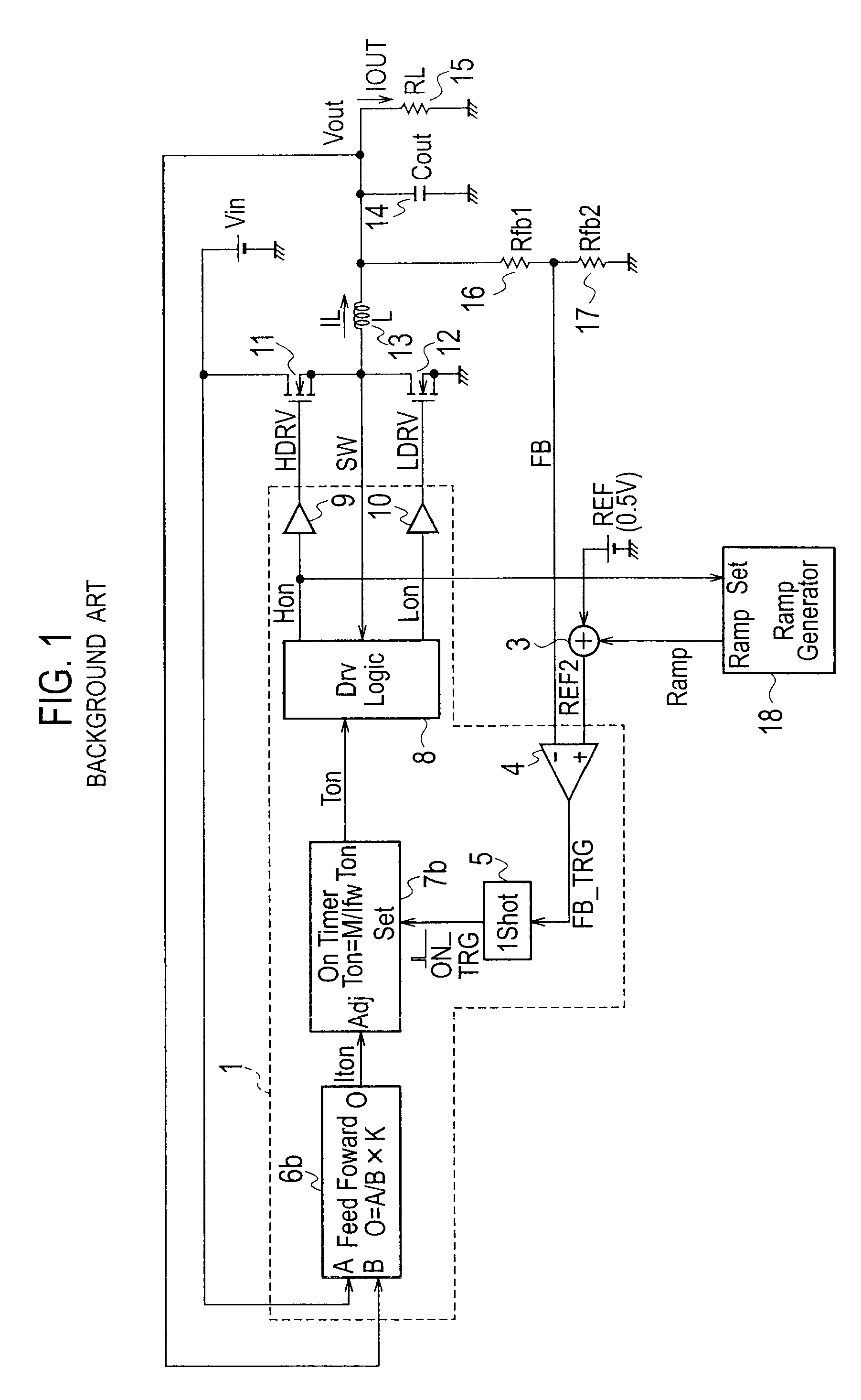
A switching power source apparatus according to Embodiment 1 of the present invention will be explained with reference to FIGS. 3 to 12. Parts of the switching power source apparatus of Embodiment 1 that are similar to those of the switching power source apparatus of the related art illustrated in FIG. 1 are represented with like reference numerals to avoid a repetition of explanation.
In FIG. 3, the switching power source apparatus according to Embodiment 1 includes a first feedback controller 1, a second feedback controller 2, a superposing circuit 3, a high-side MOSFET 11, a low-side MOSFET 12, an inductor 13, an output smoothing capacitor 14, an output load 15, and feedback resistors 16 and 17.
The first feedback controller 1 includes a feedback comparator 4, a one-shot circuit 5, a feedforward circuit 6, an ON timer 7, a drive logic 8, a high-side driver 9, and a low-side driver 10.
The second feedback controller 2 includes a ramp generator 18, a sample and hold circuit 19, an err...
embodiment 2
FIG. 13 is a circuit diagram illustrating a switching power source apparatus according to Embodiment 2 of the present invention. Embodiment 2 differs from Embodiment 1 of FIG. 3 in that Embodiment 2 employs a superposing circuit 3b whose configuration and connected location are different from those of the superposing circuit 3 of Embodiment 1.
The superposing circuit 3b corresponds to the second superposing circuit stipulated in the claims. The superposing circuit 3b generates a third ramp signal having a negative inclination corresponding to the amplitude and frequency of a ramp signal Ramp generated by a ramp generator 18 and superposes the third ramp signal on a feedback signal FB to generate a second superposed signal FB2.
FIG. 14 is a circuit diagram illustrating the details of the superposing circuit 3b. In FIG. 13, the superposing circuit 3b includes an npn transistor 31b, a pnp transistor 32b, a resistor 33b, n-channel MOSFETs 34b and 35b, a resistor 38b, and a constant curren...
PUM
 Abstract
Description
Claims
Application Information


