Diode circuit

a diode circuit and diode technology, applied in the direction of instruments, measurement using ac-dc conversion, pulse technique, etc., can solve the problems of high difficulty in setting the concentration of dopant and diffusion depth to any given designed valu

Inactive Publication Date: 2011-12-15
PANASONIC CORP
View PDF3 Cites 18 Cited by
  • Summary
  • Abstract
  • Description
  • Claims
  • Application Information

AI Technical Summary

Benefits of technology

[0029]According to this structure, the first and the second transistors may have their gate terminals connected each other and their source terminals (or their drain terminals) connected each other. This structure also allows the operational amplifier to form a negative feedback loop, so that the drain current of the second transistor makes the reference voltage and the leak current setting value equal. Hence the gate voltage generating circuit can correctly generate a gate voltage near a threshold voltage, which contributes to bringing the forward voltage to near 0 V.
[0030]The present invention can achieve ideal diode characteristics which observe an enough reverse breakdown voltage, and whose forward voltage is nearly 0 V.

Problems solved by technology

These conventional techniques have problems below.
Thus it is highly difficult to set the dopant concentration and diffusion depth to any given designed value.

Method used


Image

  • Diode circuit
  • Diode circuit
  • Diode circuit

Examples


embodiment 1

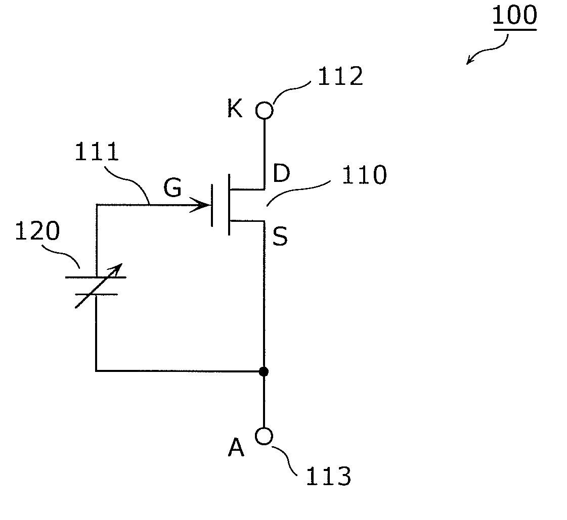
[0044]A diode circuit (an active diode) according to Embodiment 1 of the present invention includes the following: a transistor which has (i) a gate terminal, (ii) a drain terminal connected to one of an anode terminal and a cathode terminal, and (iii) a source terminal connected to the other one of the anode terminal and the cathode terminal; and a gate voltage generating circuit which delivers a gate voltage to the gate terminal. Here the gate voltage is adjusted to be equal to a threshold voltage of the transistor. The gate voltage generating circuit is not connected to the cathode terminal but is provided between the anode terminal and the gate terminal.

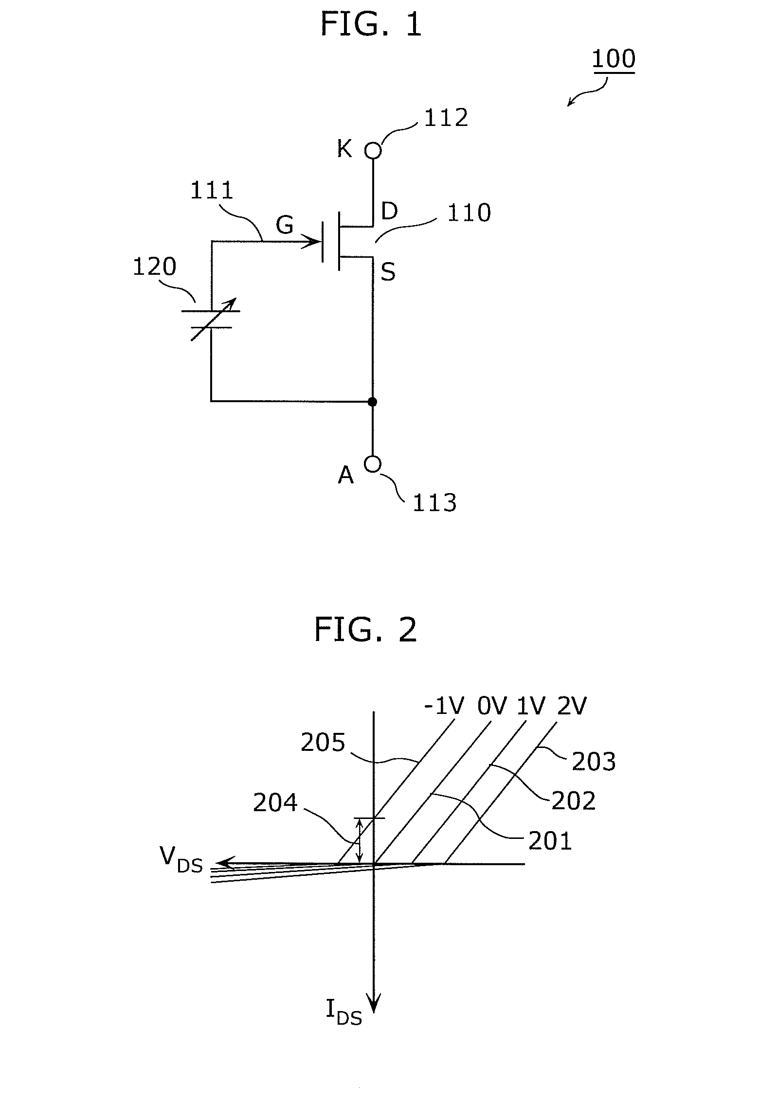
[0045]FIG. 1 exemplifies a diode circuit (an active diode 100) according to Embodiment 1 of the present invention. The active diode 100 has an anode terminal A and a cathode terminal K. When a forward voltage is applied between the anode terminal A and the cathode terminal K, a current runs from the anode terminal A to the cathod...

embodiment 2

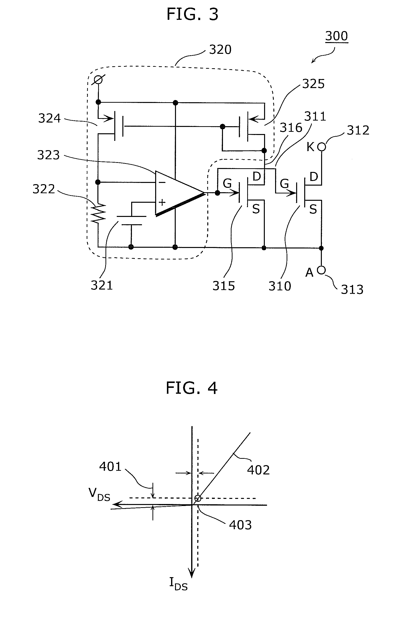
[0062]A diode circuit (an active diode) according to Embodiment 2 of the present invention includes the following: A second transistor having a gate terminal and a source terminal respectively connected to the gate terminal and the source terminal of the first transistor, the source terminals which are connected to an anode terminal; and a gate voltage generating circuit which delivers a gate voltage to the gate terminal of the first transistor and to the gate terminal of the second transistor, the gate voltage which is adjusted to be equal to a threshold voltage of the first transistor. The gate voltage generating circuit includes the following: A reference voltage source which generates a reference voltage; a resistor which generates a voltage for a drain current that runs into the second transistor; and an operational amplifier which has a positive input terminal that receives the reference voltage, a negative input terminal that receives the voltage generated by the resistor, an...


PUM


Abstract

The present invention introduces a diode circuit which achieves ideal diode characteristics which observe an enough reverse breakdown voltage, and whose forward voltage is nearly 0 V. An active diode has an anode terminal and a cathode terminal. The active diode includes a transistor which has a gate terminal, a drain terminal connected to one of the anode terminal and the cathode terminal, and a source terminal connected to the other one of the anode terminal or the cathode terminal; and a gate voltage generating circuit which delivers a gate voltage to the gate terminal, the gate voltage being adjusted to be equal to a threshold voltage of the transistor.

Description

BACKGROUND OF THE INVENTION[0001](1) Field of the Invention[0002]The present invention relates to diode circuits and, in particular, to a diode circuit which achieves diode characteristics with a current conducted in one direction so as to block a current in the opposite direction, using a transistor.[0003](2) Description of the Related Art[0004]To improve characteristics of diodes, either dedicated semiconductor devices or active diodes have been utilized. The active diodes are diode circuits which improve the diode characteristics using a circuit including an active device such as a transistor.[0005]Among the dedicated semiconductor devices, well-known devices are the ones utilizing a pn-junction on a silicon substrate and the ones utilizing the Schottky barrier junction. With a use of the pn-junction, a dedicated semiconductor device is formed of p-type impurities and n-type impurities diffusing into the silicon substrate and contacting each other. With a use of the Schottky barr...

Claims


Application Information

Patent Timeline
Patent Type & Authority Applications(United States)
IPC IPC(8): H02M7/217
CPCH02M1/083H02M2001/0048H03K2017/307Y02B70/1491H03K17/302H02M1/0048Y02B70/10
Inventor NAKAMURA, NAOYUKIMIYACHI, HIROYUKI
Owner PANASONIC CORP
Why Eureka
Try Eureka