Composite film and semiconductor light emitting device using the same

Inactive Publication Date: 2011-12-22
NITTO DENKO CORP
View PDF14 Cites 95 Cited by
  • Summary
  • Abstract
  • Description
  • Claims
  • Application Information

AI Technical Summary

Benefits of technology

[0058]In addition, when the adhesive layer or the pressure-sensitive adhesive layer has a storage elastic modulus at 25° C. of 1.0×10⁶ Pa or less and has a storage elastic modulus at 25° C. of 1.0×10⁶ Pa or more after subjected to a heating treatment at 200° C. for 1 hour, adhesion properties are further improved.
[0059]In the semiconductor light emitting device of the invention, since the composite film is provided in a state that the wavelength conversion layer faces to the light extraction direction of the semiconductor light emitting device and the excitation light from the LED enters to the path of the excitation light, the emitted light from the LED enters only into the wavelength conversion layer through the path. Moreover, the diffusive reflection resin is formed with patterning so that not only the emitted light from the LED but also the emitted light from the wavelength conversion layer are efficiently extracted. Therefore, the semi

Problems solved by technology

However, since a contrivance is not made with focusing the back scattering light C particularly in the color conversion layer and from the viewpoint of enhancing the extraction efficiency, the effect is restricted.
Moreover, Patent Documents 5 and 6 disclose methods of conveniently forming the color conversion layer by using a phosphor sheet or tape, but no contrivance for enhancing the light extraction efficiency is made.
However, when the transmitta

Method used


Image

  • Composite film and semiconductor light emitting device using the same
  • Composite film and semiconductor light emitting device using the same
  • Composite film and semiconductor light emitting device using the same

Examples


example 1

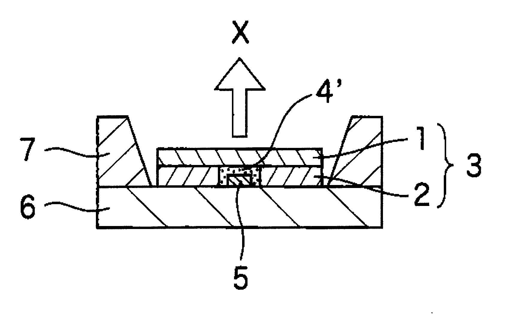
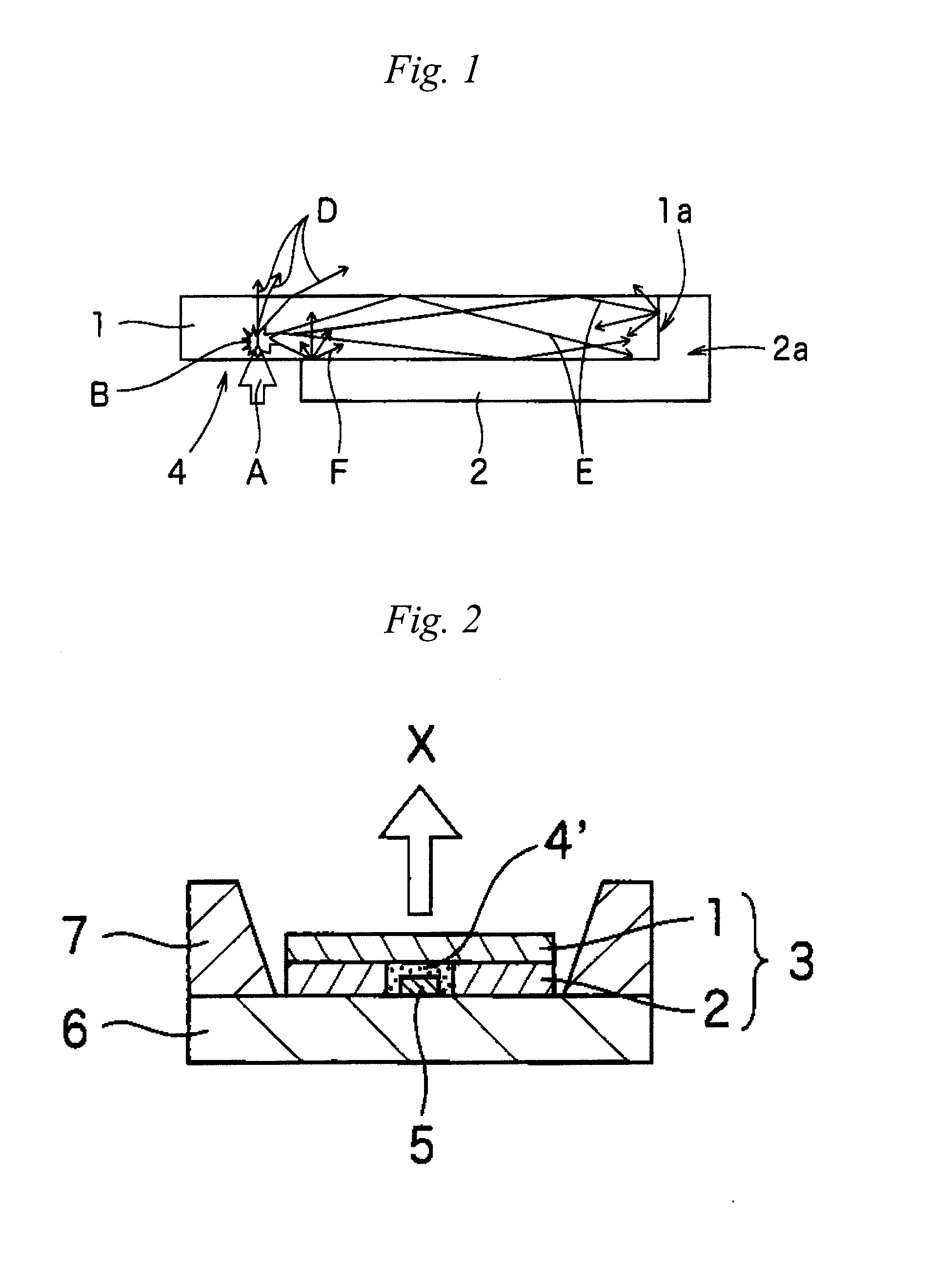
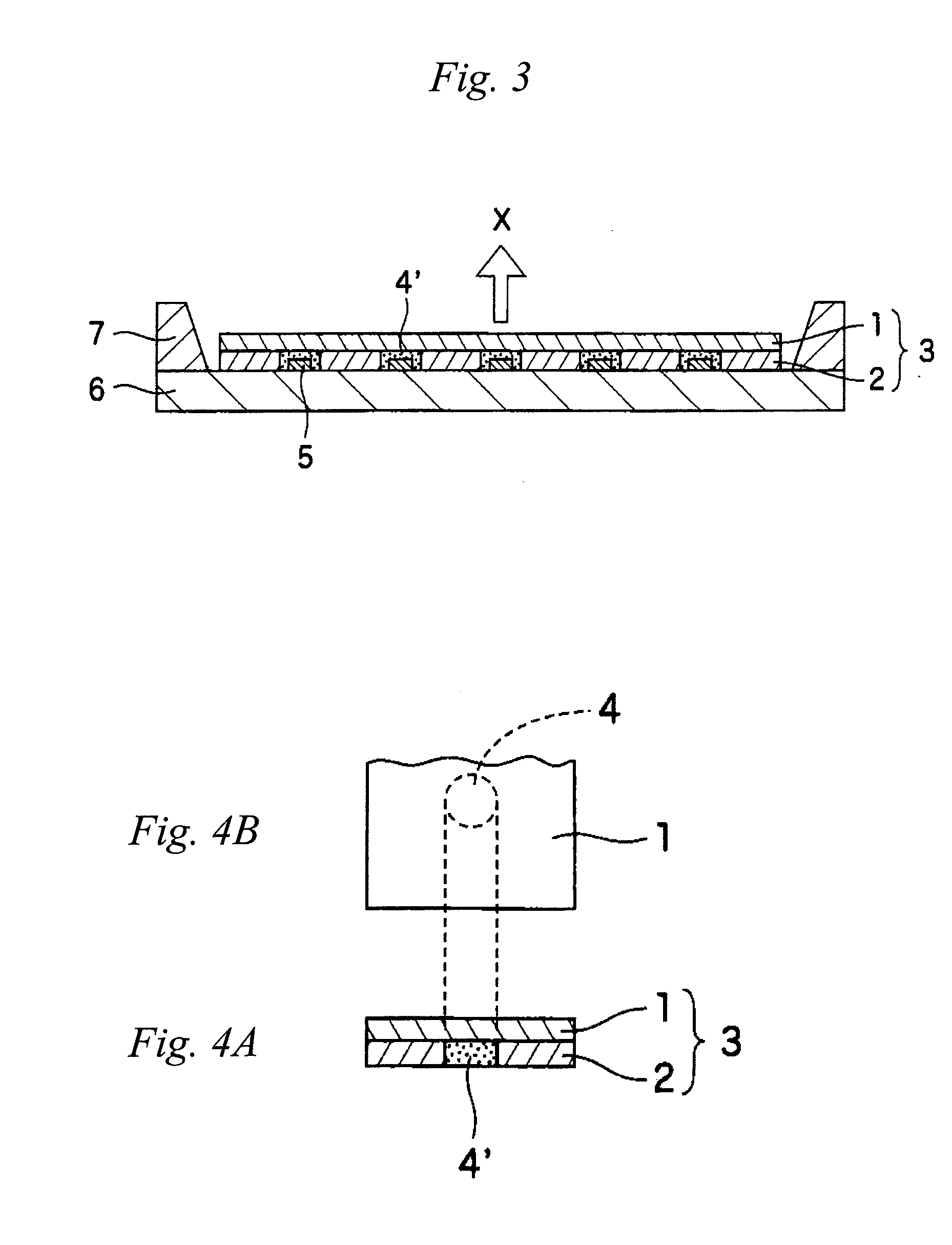
[0174]The resin composition (white resin solution) for diffusive reflection resin layer formation was applied on a PET (polyethylene terephthalate) film in a thickness of about 300 μm using an applicator and was cured by heating at 100° C. for 1 hour and at 150° C. for 1 hour, thereby forming a diffusive reflection resin layer. The diffusive reflection resin layer could be easily peeled from the PET film by curing. Then, using a round puncher (trade name: Small-Diameter Hole punches, item No. 5 / 64″3424A31 manufactured by McMASTER-CARR Company) and a rubber hammer, four holes each having a diameter of about 2 mm were punched out at intervals of 4 mm in accord with the LED-mounted pattern of the four-blue-LEDs mounted type in FIG. 18. Subsequently, after the phosphor plate (YAG plate) prepared previously was diced into a size of 10 mm×10 mm, a silicone elastomer (item No. KER 2500 manufactured by Shin-Etsu Silicone) was applied on one surface thereof using a spatula in a thickness of ...

example 2

[0176]In Example 1, a thermosetting gel-form silicone resin (trade name: WACKER SilGel 612 manufactured by Wacker AsahiKasei Silicone Co., Ltd.) was filled and applied onto the punched parts and the surface of the diffusive reflection resin layer of the resulting composite film and then cured at 100° C. for 15 minutes, thereby obtaining a composite film (see FIG. 9). The thickness of the gel-form silicone resin layer (adhesive layer) applied on the diffusive reflection resin layer was about 100 μm.

[0177]A four-blue-LEDs mounted type element was arranged. The composite film was placed while attaching with softly pushing the film so that the four punched parts were matched to the four positions on which four LED chips had been mounted, respectively and then the gel-form silicone resin was cured at 100° C. for 15 minutes, thereby preparing an LED element for test.

example 3

[0181]An LED element for test was prepared in accordance with Example 1 except that a sixteen-blue-LEDs mounted type element (see FIG. 19) was used instead of the four-blue-LEDs mounted type element (see FIG. 18).

[0182]The resin composition (white resin solution) for diffusive reflection resin layer formation was applied on a PET (polyethylene terephthalate) film in a thickness of about 300 μm and was cured by heating at 100° C. for 1 hour and at 150° C. for 1 hour, thereby forming a diffusive reflection resin layer. Then, using a round puncher (trade name: Small-Diameter Hole punches, item No. 5 / 64″3424A31 manufactured by McMASTER-CARR Company) and a rubber hammer, the diffusive reflection resin layer prepared by application on the PET film and curing was punched out to make sixteen holes having a diameter of about 2 mm at intervals of 4 mm in accord with the LED-mounted pattern of the sixteen-blue-LEDs mounted type in FIG. 19. Subsequently, a silicone elastomer (item No. KER 2500 ...


PUM

PropertyMeasurementUnit
Temperatureaaaaaaaaaa
Timeaaaaaaaaaa

Abstract

The present invention relates to a composite film including a wavelength conversion layer and a diffusive reflection resin layer in a laminated state and being used in a semiconductor light emitting device, in which the wavelength conversion layer contains a phosphor material which absorbs a part or all of excitation light and is excited to emit visible light in a wavelength region longer than a wavelength of the excitation light, the diffusive reflection resin layer is selectively formed with patterning on one surface of the wavelength conversion layer, and a region on the one surface of the wavelength conversion layer where the diffusive reflection resin layer is not formed with patterning is a path of the excitation light which excites the phosphor material in the wavelength conversion layer.

Description

FIELD OF THE INVENTION[0001]The present invention relates to a composite film and a semiconductor light emitting device using the same. More particularly, it relates to a composite film which can be suitably used in a semiconductor light emitting device having a light emitting diode (LED), particularly a blue LED or a near-ultraviolet LED and converting the wavelength of a part or all of emission of the LED to emit white light or other visible light, and a semiconductor light emitting device using the same.BACKGROUND OF THE INVENTION[0002]As one of visible light sources for displaying or lighting, there is a light emitting device using a blue LED or a near-ultraviolet LED based on a gallium nitride-based compound semiconductor such as GaN, GaAlN, InGaN, or InAlGaN. In the light emitting device, white light or other visible light emission can be obtained by using a phosphor material which absorbs a part or all of the emission from the LED as excitation light and converts the waveleng...

Claims


Application Information

Patent Timeline
IPC IPC(8): H01L33/50B32B3/00
CPCH01L33/505H01L33/507H01L33/54Y10T428/24802H01L2224/8592H01L33/60H01L2224/13H01L2924/181H01L2924/00012H01L33/50H01L33/52
Inventor ITO, HISATAKANAKAMURA, TOSHITAKAFUJII, HIRONAKA
Owner NITTO DENKO CORP
Why Eureka
Try Eureka