
Method of simulation and design of a semiconductor device

a semiconductor and computer simulation technology, applied in the field of semiconductor devices, can solve the problems of loss of precision and instability of numerical methods, time-consuming and associated costs, and conventional methods that do not work well for wide band gaps, so as to reduce external bias and reduce external bias

Inactive Publication Date: 2011-12-22
CROSSLIGHT SOFTWARE
View PDF2 Cites 35 Cited by
  • Summary
  • Abstract
  • Description
  • Claims
  • Application Information

AI Technical Summary

Benefits of technology

[0018](d) reducing the external bias in the biased wide-bandgap model so as to gradually change said biased wide-bandgap model by decreasing the external bias and computing a model of the wide-bandgap semiconductor device.

Problems solved by technology

Simulation is used for prototyping and validation of new design ideas, and at least partially replaces wafer processing and testing, which are time consuming and have associated costs.
However, conventional methods do not work well for wide bandgap semiconductor devices in particular because the transmission probability by thermionic emission process at heterojunctions declines exponentially with the barrier height, which causes loss of precision and instability of numerical methods.
Another issue is the intrinsic carrier density which is the population of electrons and holes in an undoped semiconductor at equilibrium.
Therefore, larger bandgaps and low temperatures are associated with lower intrinsic densities and very low electric current values, which creates the problem of enforcing the current continuity within the limits of fixed precision arithmetic on a computer.

Method used


Image

  • Method of simulation and design of a semiconductor device
  • Method of simulation and design of a semiconductor device
  • Method of simulation and design of a semiconductor device

Examples


Embodiment Construction

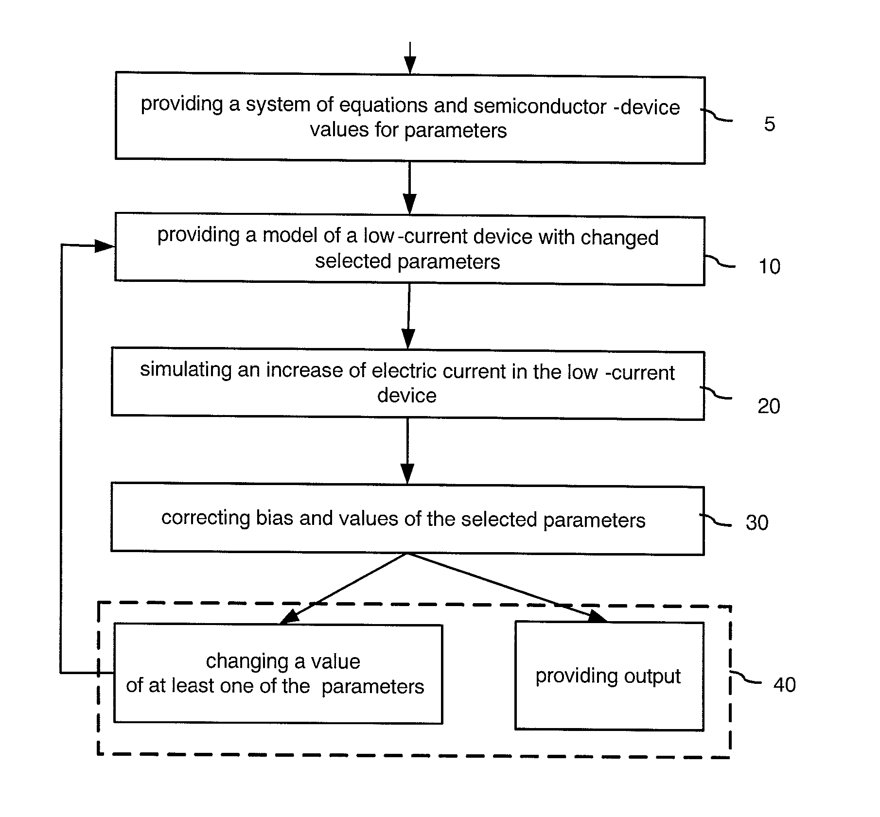
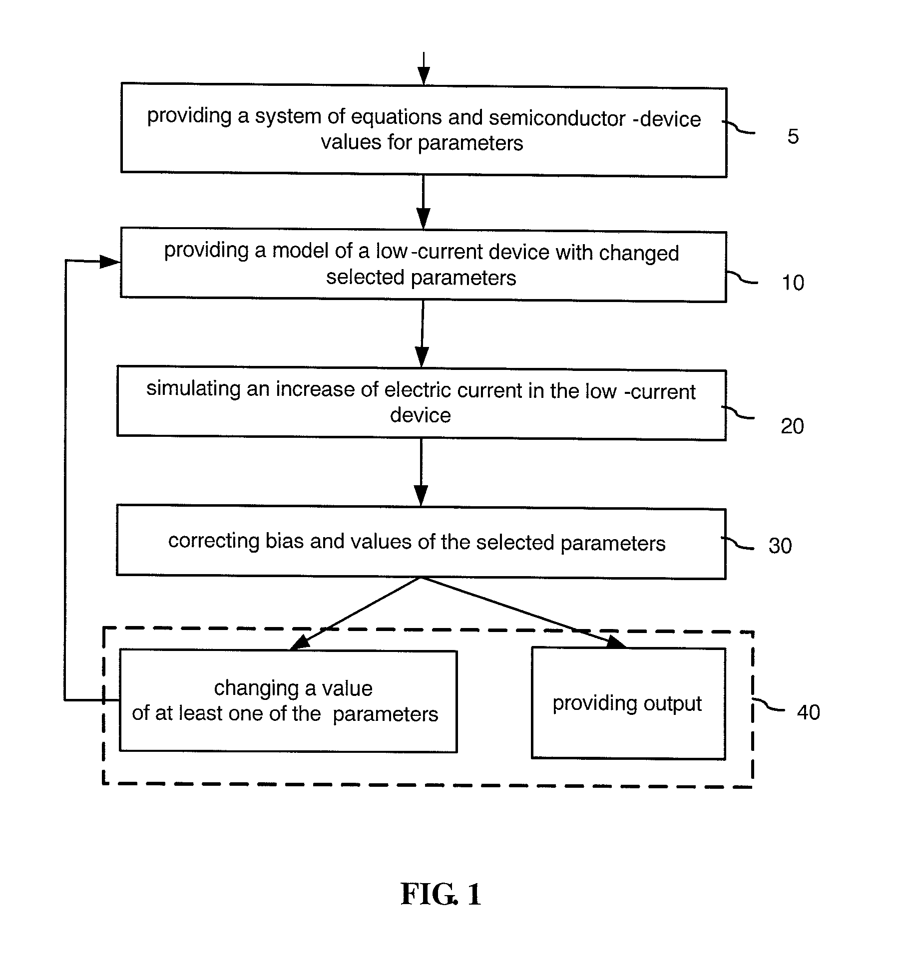
[0049]A method of simulation a semiconductor device employs a device substitution technique, starting with a model of a device which is structurally similar to the target device but has some material parameters altered to make its simulation easier. By way of example for a wide-bandgap device a substitution device would have a reduced bandgap. The method simulates applying an external bias, such as a bias voltage, to the substitution device and, after the electric current increases, the model is modified by gradually correcting the previously changed material parameters so as to arrive at the target device being simulated.

[0050]In other words, the method directs simulation steps from the initial approximation, which is the substitution device, not to the target device as it is done in conventional methods, but in detour through the substitution device having high current values. The detour allows to bypass a region where numerical convergence is very slow and / or difficult and eventu...


PUM


Abstract

The invention relates to a method of simulation of semiconductor devices, such as wide-bandgap devices. The method employs a device substitution technique and involves simulation of a device which is structurally similar to the target device, and for which it is relatively easy to compute a model. Such a device may have a reduced material bandgap or a different doping / fixed-charge concentration. Based on the model of the simplified device, a model of the device under consideration is produced via a sequence of simulation steps, wherein simulated intermediate devices eventually transform into the target device for which a model is sought.

Description

CROSS-REFERENCE TO RELATED APPLICATIONS[0001]The present invention claims priority from U.S. Patent Application No. 61 / 355,191 filed Jun. 16, 2010, which is incorporated herein by reference for all purposes.TECHNICAL FIELD[0002]The present invention relates to semiconductor devices and more specifically to methods of computer simulation of semiconductor devices.BACKGROUND OF THE INVENTION[0003]Semiconductor devices have a wide variety of applications such as photovoltaics (solar cells), telecommunications (laser diodes), consumer products (high-brightness light-emitting diodes), and computers (transistors). The continued development of semiconductor devices drives many technological improvements in other fields.[0004]The computer-based simulation of semiconductor devices is an important component in the design process. Simulation is used for prototyping and validation of new design ideas, and at least partially replaces wafer processing and testing, which are time consuming and have...

Claims


Application Information

Patent Timeline
IPC IPC(8): G06F17/50G06F17/11
CPCG06F17/5045G06F17/5036G06F30/367G06F30/30
Inventor LI, ZHANMING
Owner CROSSLIGHT SOFTWARE
Learn More