

Method for sealing two elements by low temperature thermocompression
a technology of thermocompression and sealing elements, applied in the field of assembly of two elements, can solve the problems of incompatibility with many microelectronic applications, limited type of sealing, and difficulty in implementing it for packaging microsystems, and achieve the effect of preventing potential short circuits
- Summary
- Abstract
- Description
- Claims
- Application Information
AI Technical Summary
Benefits of technology
Problems solved by technology
Method used
Image

Examples
Embodiment Construction
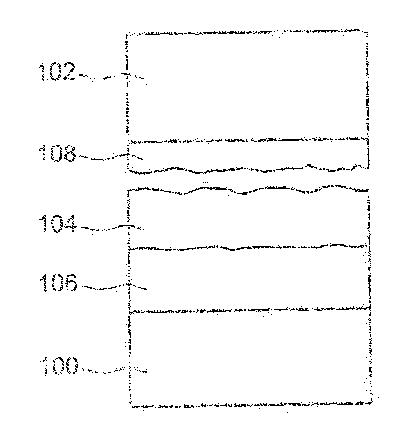
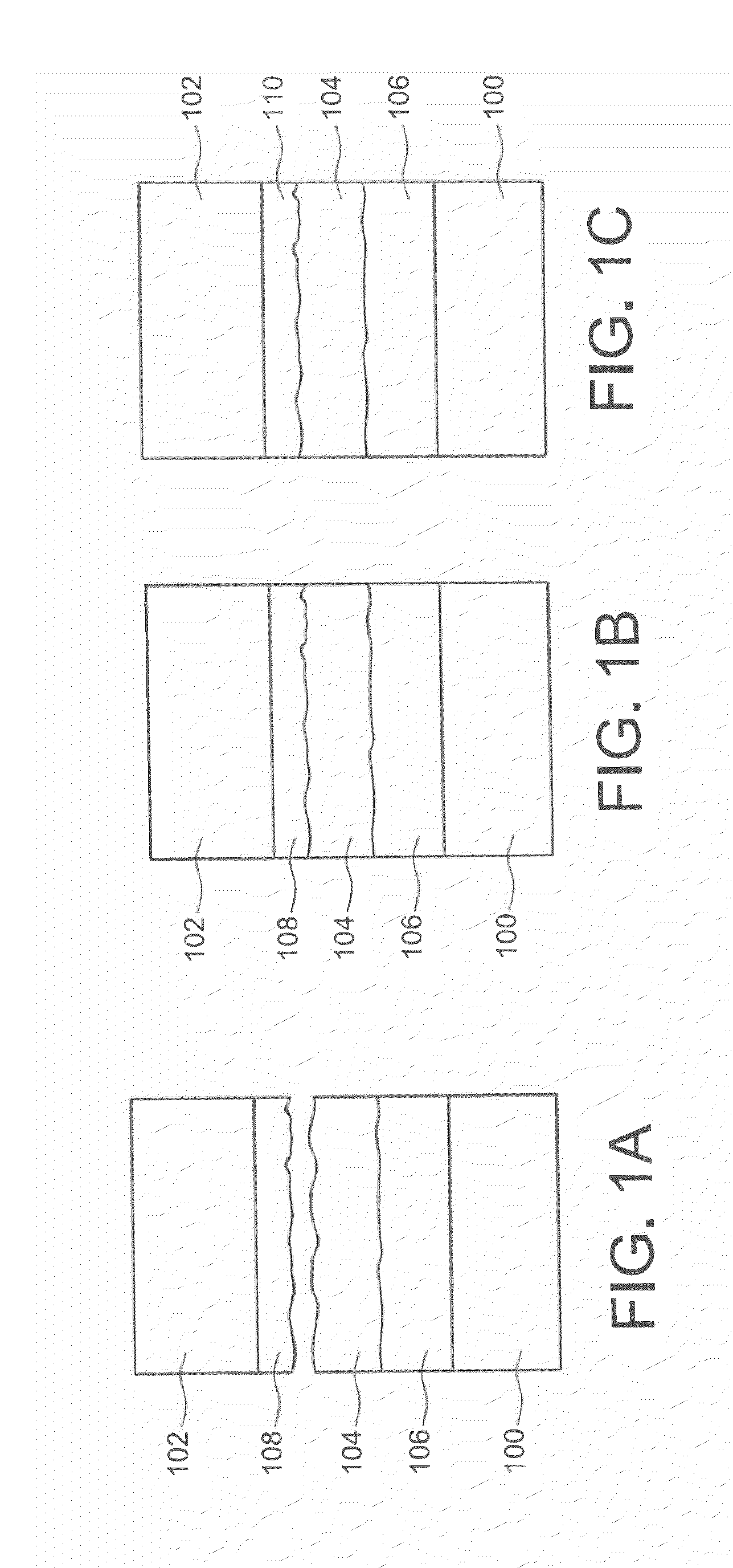
[0063]Reference is first made to FIGS. 1A to 1C, which diagrammatically show the steps of a method for sealing two substrates 100 and 102 according to a particular embodiment.
[0064]As shown in FIG. 1A, a layer 104 of a first sealing material is made on a face of the first substrate 100. Although it is possible to make the layer 104 directly against the first substrate 100, it is also possible, as shown in FIG. 1A, for the production of the layer 104 to lead to the formation of one or more other phases 106 on the first substrate 100.
[0065]A layer 108 of a second sealing material is made on a face of the second substrate 102. The second sealing material is of a different nature than the first sealing material. The two sealing materials are chosen such that the components of the phase(s) of these materials are able to react together to form at least one other phase.
[0066]As shown in FIG. 1B, the layer 104 is then put in contact and pressure against the layer 108. This assembly is done ...
PUM
| Property | Measurement | Unit |
|---|---|---|
| temperature Tc | aaaaa | aaaaa |
| pressure | aaaaa | aaaaa |
| temperature | aaaaa | aaaaa |
Abstract
Description
Claims
Application Information