Apparatuses and methods for atomic layer deposition

a technology of atomic layer and apparatus, which is applied in the direction of couplings, braking systems, transportation and packaging, etc., can solve the problems of many limitations of pe-ald processes, slow process deposition rate, and inability to meet the requirements of atomic layer deposition, etc., to achieve better uniformity, lower hole density, and high hole density

Active Publication Date: 2012-01-05
APPLIED MATERIALS INC
View PDF99 Cites 15 Cited by
  • Summary
  • Abstract
  • Description
  • Claims
  • Application Information

AI Technical Summary

Benefits of technology

[0019]In other embodiments, the showerhead plate contains a lower hole density at the center of the showerhead plate and a higher hole density at the edge of the showerhead plate. These lower / higher hole densities help to direct more nitrogen plasma or nitrogen radicals to edge of the showerhead plate for better uniformity as gas inlet was located in the center position. In addition, gradual change of hole sizes from small to large at center to edge of showerhead plate. In another aspect, the showerhead plate may contain holes with a diameter within a range from about 0.08 inches to about 0.13 inches. This hole size reduces the recombination of nitrogen radicals, which improves the film properties.

Problems solved by technology

While conventional chemical vapor deposition (CVD) has proved successful for device geometries and aspect ratios down to 0.15 μm, the more aggressive device geometries require an alternative deposition technique.
While thermal ALD processes work well to deposit some materials, the processes often have a slow deposition rate.
Therefore, fabrication throughput may be impacted to an unacceptable level.
While PE-ALD processes overcome some of the shortcomings of thermal ALD processes due to the high degree of reactivity of the reactant radicals within the plasma, PE-ALD processes have many limitations.
PE-ALD process may cause plasma damage to a substrate (e.g., etching), be incompatible with certain chemical precursors and require additional hardware.

Method used


Image

  • Apparatuses and methods for atomic layer deposition
  • Apparatuses and methods for atomic layer deposition
  • Apparatuses and methods for atomic layer deposition

Examples


Embodiment Construction

Deposition Chamber

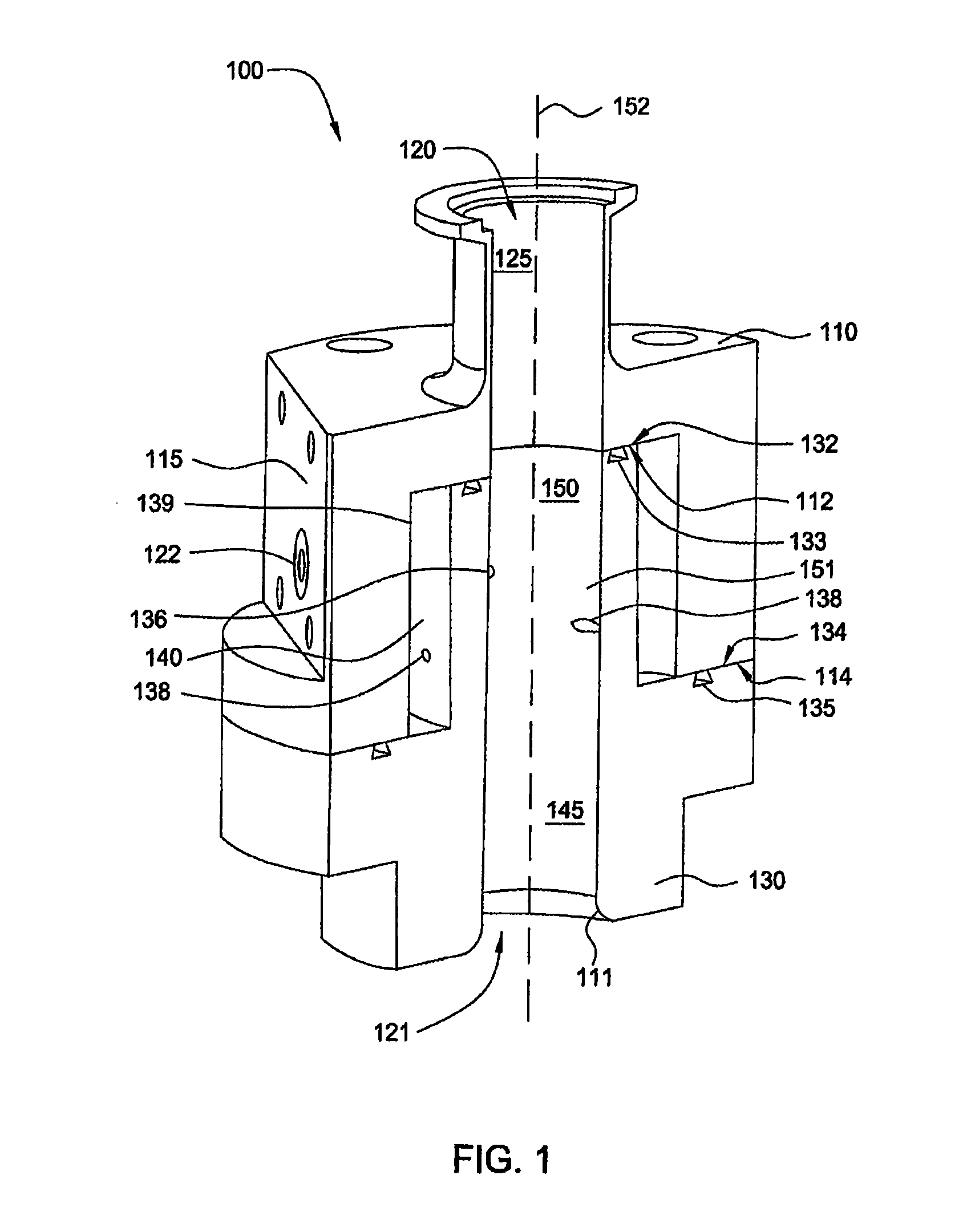
[0044]Embodiments of the invention provide an apparatus configured to form materials during atomic layer deposition (ALD) processes, such as a thermal ALD process or a plasma-enhanced ALD (PE-ALD) process. Other embodiments of the invention provide ALD and PE-ALD processes for forming various materials, such as titanium nitride. In some embodiments, a processing system or chamber is configured to expose a substrate to a sequence of gases and plasmas during a PE-ALD process. In one embodiment, a deposition chamber is configured to perform a PE-ALD process using a remote plasma system (RPS) for igniting the plasma. In another embodiment, the deposition chamber is configured to perform a thermal ALD process.

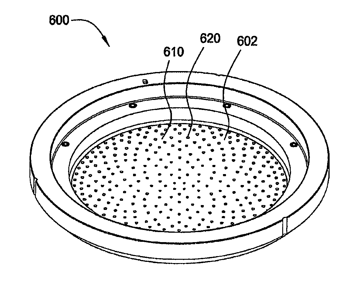
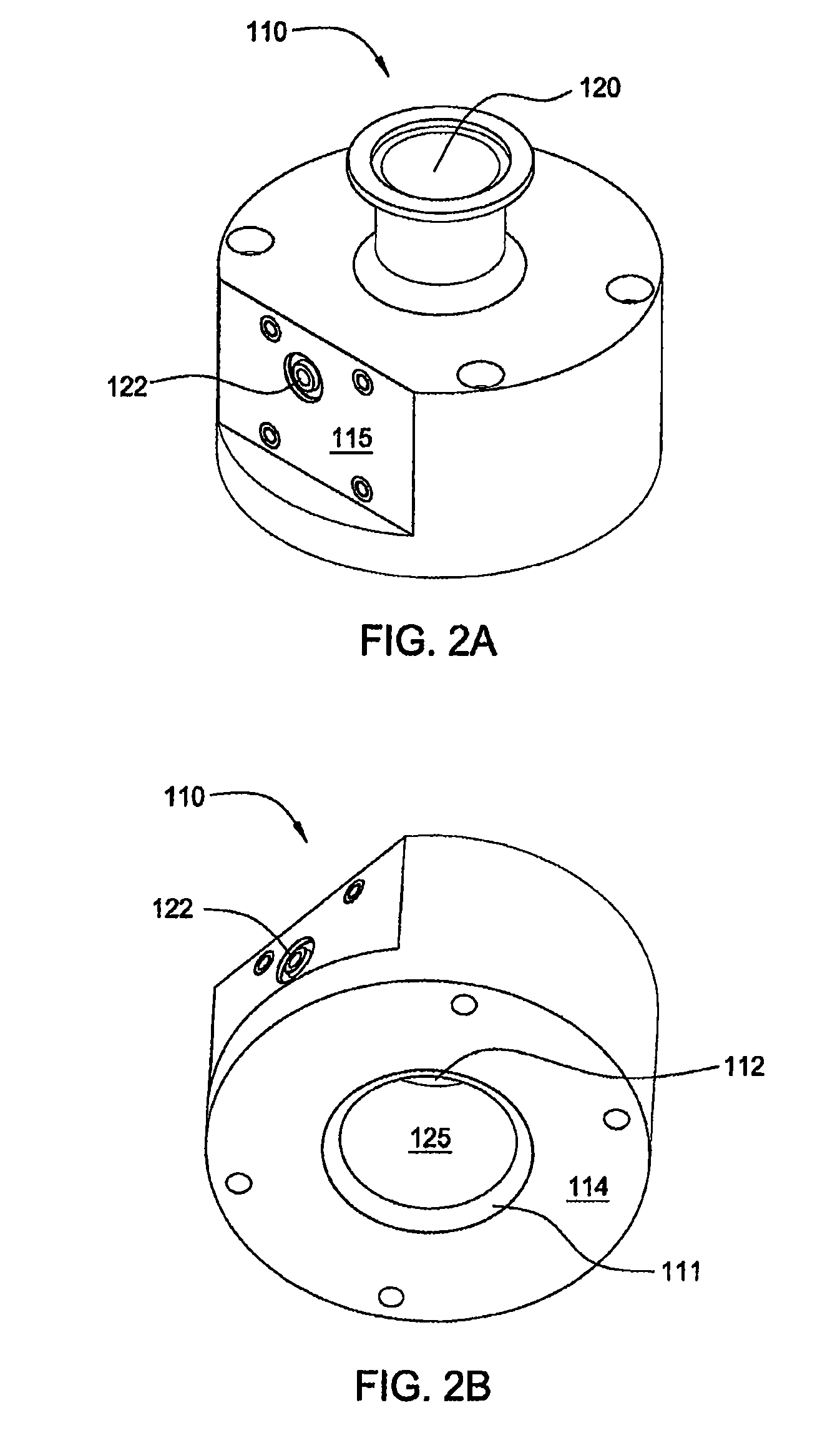
[0045]FIG. 1 depicts inlet manifold assembly 100 which may be utilized within or by thermal or plasma-enhanced ALD systems, chambers, and processes, such as described herein. Inlet manifold assembly 100 contains upper inlet manifold 110 and lower inlet manifold 130...


PUM

PropertyMeasurementUnit
diameteraaaaaaaaaa
diameteraaaaaaaaaa
diameteraaaaaaaaaa

Abstract

Embodiments of the invention provide apparatuses and methods for atomic layer deposition (ALD), such as plasma-enhanced ALD (PE-ALD). In some embodiments, a PE-ALD chamber is provided which includes a chamber lid assembly coupled with a chamber body having a substrate support therein. In one embodiment, the chamber lid assembly has an inlet manifold assembly containing an annular channel encompassing a centralized channel, wherein the centralized channel extends through the inlet manifold assembly, and the inlet manifold assembly further contains injection holes extending from the annular channel, through a sidewall of the centralized channel, and to the centralized channel. The chamber lid assembly further contains a showerhead assembly disposed below the inlet manifold assembly, a water box disposed between the inlet manifold assembly and the showerhead assembly, and a remote plasma system (RPS) disposed above and coupled with the inlet manifold assembly, and in fluid communication with the centralized channel.

Description

CROSS-REFERENCE TO RELATED APPLICATION[0001]This application is a continuation of U.S. Ser. No. 12 / 494,901 (APPM / 012913US), filed Jun. 30, 2009, which claims benefit of U.S. Ser. No. 61 / 078,321 (APPM / 012913L), filed Jul. 3, 2008, which are herein incorporated by reference in their entirety.BACKGROUND OF THE INVENTION[0002]1. Field of the Invention[0003]Embodiments of the invention generally relate to an apparatus and a method for depositing materials, and more particularly to an atomic layer deposition chamber configured to deposit a material during a plasma-enhanced process.[0004]2. Description of the Related Art[0005]In the field of semiconductor processing, flat-panel display processing or other electronic device processing, vapor deposition processes have played an important role in depositing materials on substrates. As the geometries of electronic devices continue to shrink and the density of devices continues to increase, the size and aspect ratio of the features are becoming...

Claims


Application Information

Patent Timeline
Patent Type & Authority Applications(United States)
IPC IPC(8): C23C16/455F17D1/20
CPCC23C16/4412C23C16/45536H01J37/32449C23C16/45565C23C16/4558C23C16/45544Y10T137/87265
Inventor LAM, HYMANZHENG, BOAI, HUAJACKSON, MICHAELYUAN, XIAOXIONG (JOHN)WANG, HOU GONGUMOTOY, SALVADOR P.YU, SANG HO
Owner APPLIED MATERIALS INC
Why Eureka
Try Eureka