Layout for multiple-fin SRAM cell

a sram cell and multiple-fin technology, applied in the direction of transistors, electrical apparatus, semiconductor devices, etc., can solve the problems of difficult to achieve further reduction of pitch in finfet devices, undesirable snm reduction caused by increasingly smaller transistor geometries,

Active Publication Date: 2012-01-05
ADVANCED MFG INNOVATIONS INC
View PDF1 Cites 74 Cited by
  • Summary
  • Abstract
  • Description
  • Claims
  • Application Information

AI Technical Summary

Benefits of technology

[0007]The present disclosure provides yet another embodiment of a static random access memory (SRAM) cell. The SRAM cell includes a first inverter including a first pull-up transistor (PU-1) and a first and second pull-down transistors (PD-1 and PD-2); a second inverter including a second pull-up transistor (PU-2) and a third and fourth pull-down transistors (PD-3 and PD-4), the second inverter being cross-coupled with the first inverter for data storage; a port including a first pass-gate transistor (PG-1) and a second pass-gate transistor (PG-2), the port being coupled with the first and second inverters for data access

Problems solved by technology

This reduction in SNM caused by increasingly smaller transistor geometries is undesirable.
Unfortunately, it is difficult to achieve further reductions in pitch

Method used


Image

  • Layout for multiple-fin SRAM cell
  • Layout for multiple-fin SRAM cell
  • Layout for multiple-fin SRAM cell

Examples


Embodiment Construction

[0013]It is to be understood that the following disclosure provides many different embodiments, or examples, for implementing different features of various embodiments. Specific examples of components and arrangements are described below to simplify the present disclosure. These are, of course, merely examples and are not intended to be limiting. In addition, the present disclosure may repeat reference numerals and / or letters in the various examples. This repetition is for the purpose of simplicity and clarity and does not in itself dictate a relationship between the various embodiments and / or configurations discussed.

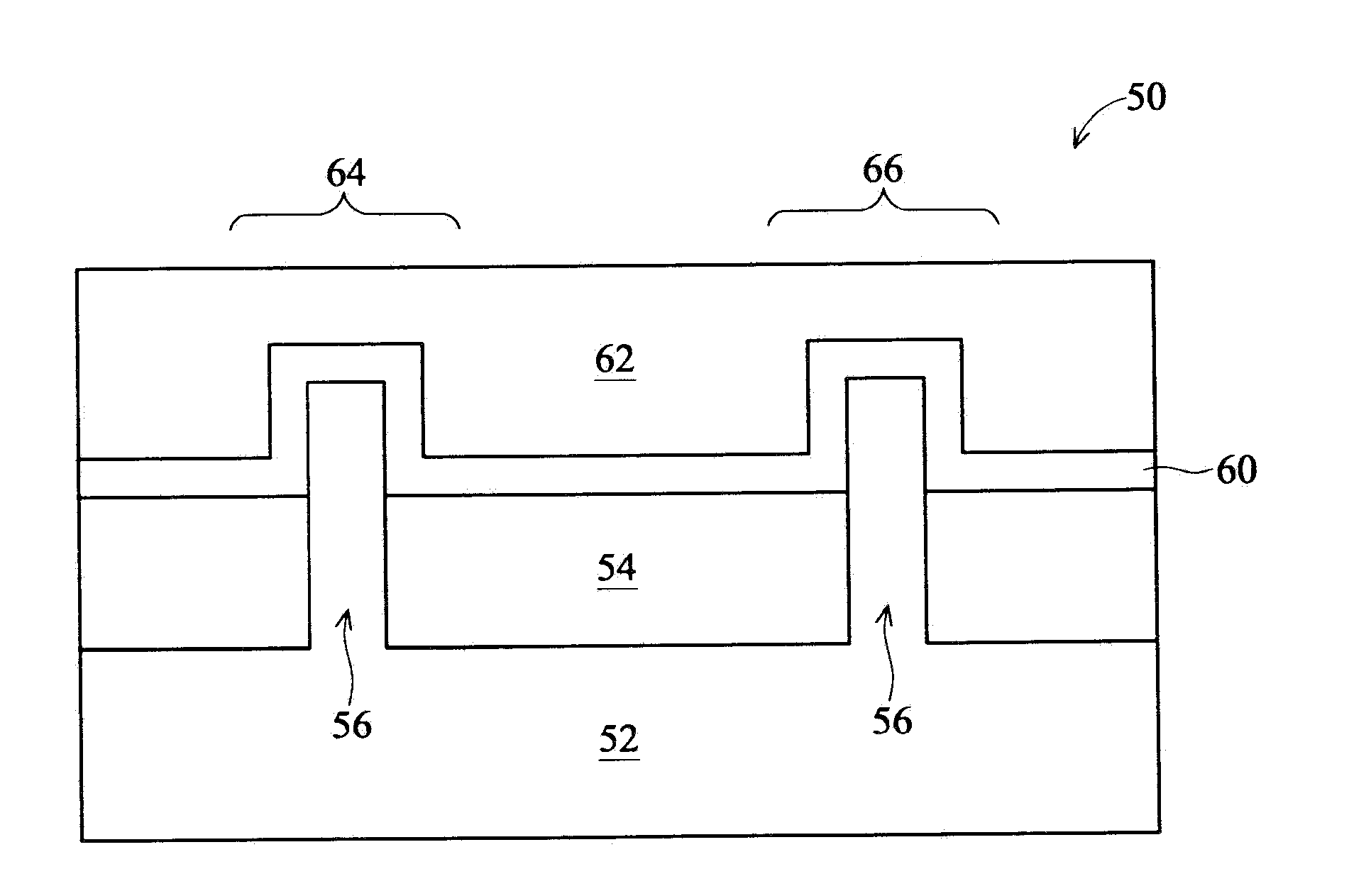
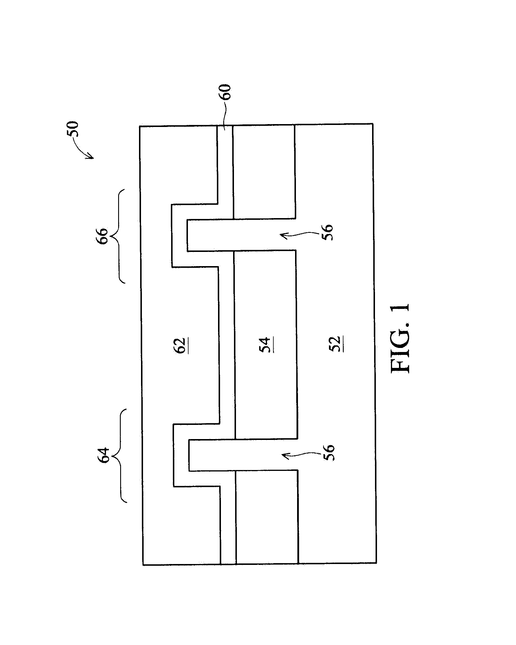
[0014]FIG. 1 is a sectional view of a semiconductor structure 50 as a portion of a SRAM cell constructed according to various aspects of the present disclosure. The semiconductor structure 50 includes a semiconductor substrate 52. The semiconductor substrate 52 includes silicon. Alternatively, the substrate includes germanium, silicon germanium or other proper semicond...


PUM


Abstract

The present disclosure provides a static random access memory (SRAM) cell. The SRAM cell includes a plurality of fin active regions formed on a semiconductor substrate, wherein the plurality of fin active regions include a pair adjacent fin active regions having a first spacing and a fin active region having a second spacing from adjacent fin active regions, the second spacing being greater than the first spacing; a plurality of fin field-effect transistors (FinFETs) formed on the plurality of fin active regions, wherein the plurality of FinFETs are configured to a first and second inverters cross-coupled for data storage and at least one port for data access; a first contact disposed between the first and second the fin active regions, electrically contacting both of the first and second the fin active regions; and a second contact disposed on and electrically contacting the third fin active region.

Description

CROSS REFERENCE[0001]The present disclosure is related to the following commonly-assigned U.S. patent applications, the entire disclosures of which are incorporated herein by reference: U.S. Ser. No. 12 / 721,476 filed Mar. 10, 2010 by the same inventor Jhon Jhy Liaw for “FULLY BALANCED DUAL-PORT MEMORY CELL” (attorney reference TSMC2009-0686); and U.S. Ser. No. 12 / 823,860 filed Jun. 25, 2010 (attorney reference TSMC2010-0192) by the same inventor Jhon Jhy Liaw for “STRUCTURE AND METHOD FOR SRAM CELL CIRCUIT”.BACKGROUND[0002]In deep sub-micron integrated circuit technology, an embedded static random access memory (SRAM) device has become a popular storage unit of high speed communication, image processing and system-on-chip (SOC) products. The amount of embedded SRAM in microprocessors and SOCs increases to meet the performance requirement in each new technology generation. As silicon technology continues to scale from one generation to the next, the impact of intrinsic threshold volt...

Claims


Application Information

Patent Timeline
IPC IPC(8): H01L29/24H01L27/088
CPCH01L21/845H01L27/1104H01L27/11H10B10/00H10B10/12H01L21/8234H01L21/8238H01L27/092
Inventor LIAW, JHON JHYSHEN, JENG-JUNG
Owner ADVANCED MFG INNOVATIONS INC
Why Eureka
Try Eureka