
Star coupler and optical multiplexer/demultiplexer

Inactive Publication Date: 2012-01-05
OKI ELECTRIC IND CO LTD
View PDF13 Cites 20 Cited by
  • Summary
  • Abstract
  • Description
  • Claims
  • Application Information

AI Technical Summary

Benefits of technology

[0008]An object of the present invention is to reduce light loss in a silicon star coupler.
[0009]Another object is to reduce light loss in an AWG optical multiplexer / demultiplexer employing silicon star couplers.
[0010]Through diligent study, the inventors have found that these objects can be achieved by providing layers of a material with a high refractive index on the sides of the optical waveguides.
[0018]When a silicon core is employed in the above star coupler and optical multiplexer / demultiplexer, the high-index layer has the effect of reducing light loss.

Problems solved by technology

An unwanted result is that much of the light propagating in the slab waveguides is lost to the outside by radiation through the spaces between the arrayed waveguides.
U.S. Pat. No. 6,973,236 (WO 2004 / 061498 A1) and Japanese Patent Application Publications No. 2006-30687, 2005-202373, 2004-325865, 2004-170627, 2004-29073, 2002-62444, 2001-159718, and 2000-147283 describe various attempts to deal with the corresponding problem in quartz waveguides, but none of the methods employed are readily applicable to an AWG with silicon waveguides.

Method used


Image

  • Star coupler and optical multiplexer/demultiplexer
  • Star coupler and optical multiplexer/demultiplexer
  • Star coupler and optical multiplexer/demultiplexer

Examples


first embodiment

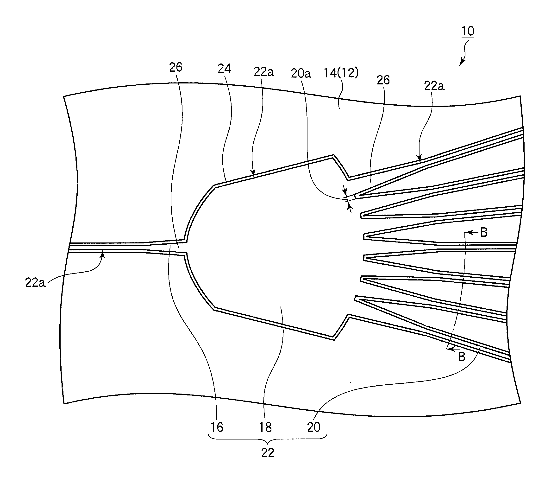
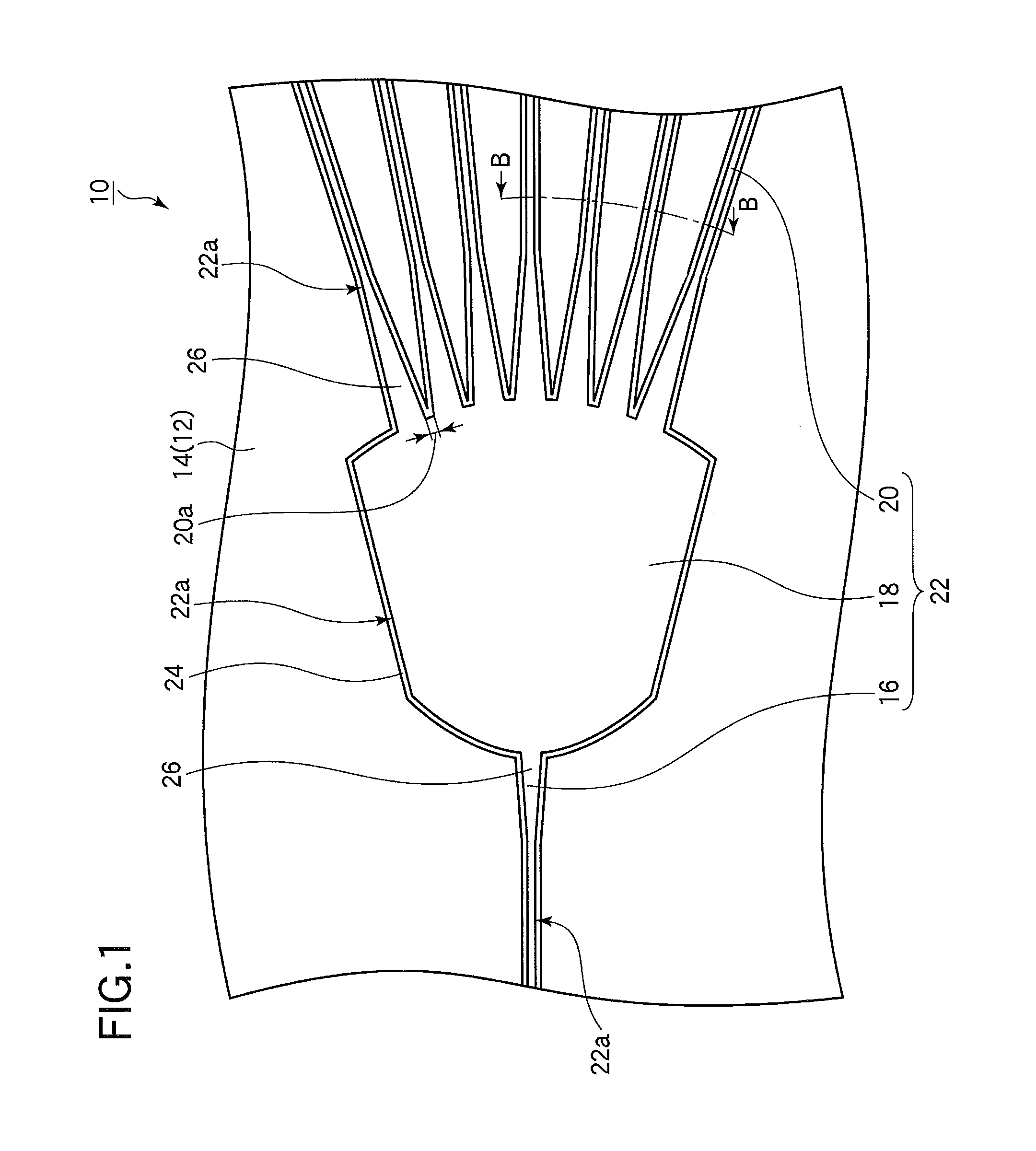
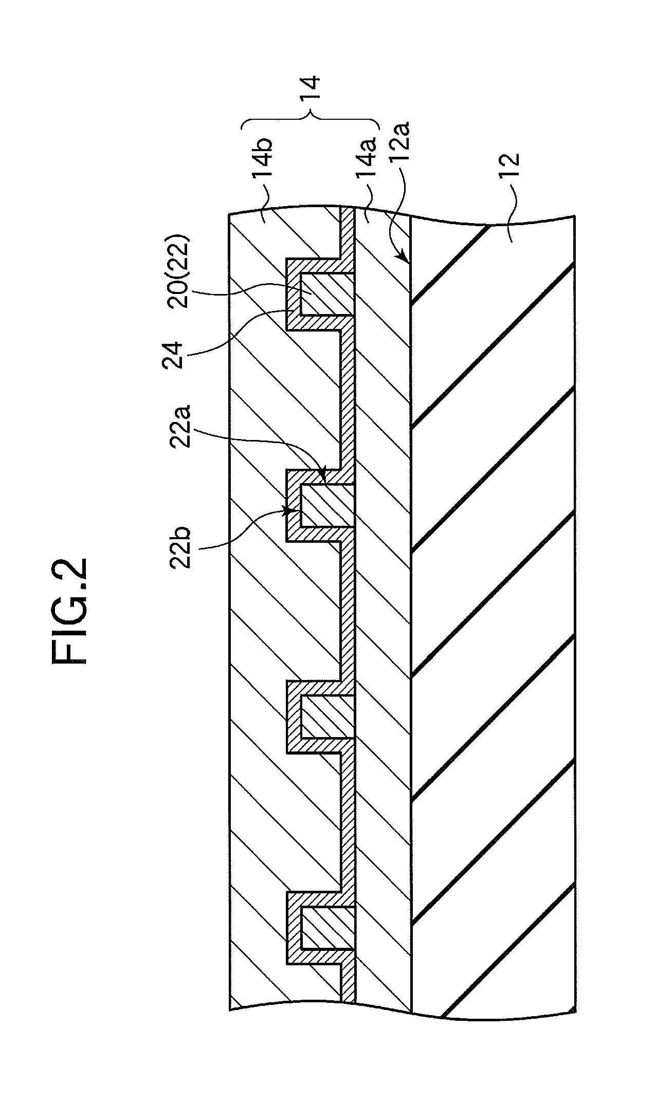
[0029]The structure of the star coupler in the first embodiment is shown in FIGS. 1 and 2. For clarity, the core in FIG. 1 is indicated by solid lines, even though it is embedded in the clad and would not be visible to the eye.

[0030]The star coupler 10 in FIGS. 1 and 2 includes a substrate 12, a clad 14 disposed on a major surface 12a of the substrate 12, and, embedded in the clad 14, an input-output optical waveguide 16, a slab optical waveguide 18, and a plurality of channel optical waveguides 20.

[0031]The input-output optical waveguide 16, slab optical waveguide 18, and channel optical waveguides 20 function as core elements in the clad 14, and will be referred to collectively below as the core 22. The sides of the core 22, more specifically the sides 22a orthogonal to the major surface 12a of the substrate, are entirely covered by a high-index layer 24. The high-index layer 24 also covers the top surface 22b of the core 22. ‘High-index’ in this specification means a refractive i...

second embodiment

[0062]The second embodiment is an AWG optical multiplexer / demultiplexer with the structure shown in schematic perspective view in FIG. 6. For clarity, the optical multiplexer / demultiplexer 60 is indicated by solid lines, even though it is embedded in the clad 14 and would not be visible to the eye.

[0063]The clad 14 in which the optical multiplexer / demultiplexer 60 is embedded is formed on the major surface 12a of a substrate 12. The optical multiplexer / demultiplexer 60 comprises a first star coupler 62 and a second star coupler 64, each similar to the star coupler 10 described in the first embodiment. The optical multiplexer / demultiplexer 60 further comprises arrayed waveguides 661 to 664 that interconnect the first star coupler 62 and the second star coupler 64.

[0064]The first star coupler 62 has a single input optical waveguide 68 identical to the input-output optical waveguide in the first embodiment, a slab optical waveguide 76 identical to the slab optical waveguide in the firs...


PUM


Abstract

A star coupler includes a core embedded in a clad on a major surface of a substrate. The refractive index of the core differs by at least 40% from the refractive index of the clad. The core includes a slab optical waveguide, at least one input-output optical waveguide connected to the slab optical waveguide, and an array of channel optical waveguides connected to the slab optical waveguide. The star coupler also includes a high-index layer having a refractive index intermediate between the refractive indexes of the clad and core, covering the sides of the core orthogonal to the major surface of the substrate. The high-index layer reduces light loss.

Description

BACKGROUND OF THE INVENTION[0001]1. Field of the Invention[0002]The present invention relates to a star coupler and to an optical multiplexer / demultiplexer of the arrayed waveguide grating type including the star coupler.[0003]2. Description of the Related Art[0004]The use of silicon (Si) as an optical waveguide material is a technology that has gained attention as a way of mass-producing optical elements and reducing their size. One known type of silicon optical element is an optical multiplexer / demultiplexer. This type of element is used in optical subscriber telecommunication systems to multiplex light of different wavelengths into a single optical fiber and to separate the different wavelengths of light exiting the fiber.[0005]Among the various optical multiplexer / demultiplexer structures, recently there has been much interest in optical multiplexer / demultiplexers employing an arrayed waveguide grating (AWG) structure, which combines good multiplexing and demultiplexing characte...

Claims


Application Information

Patent Timeline
IPC IPC(8): G02B6/26
CPCG02B6/12011G02B6/2813G02B6/125G02B6/12014
Inventor OKAYAMA, HIDEAKI
Owner OKI ELECTRIC IND CO LTD
Learn More