Stress detection within an integrated circuit having through silicon vias

a stress detection and integrated circuit technology, applied in the direction of electrical/magnetic measuring arrangements, using electrical/magnetic means, liquid/fluent solid measurements, etc., can solve the problems of incorrect circuitry operation, high mechanical strain, and mechanical strain within the wafer layer, so as to improve the efficiency of managing the operating parameters of the integrated circuit, improve the effect of performance and reliable functioning

Active Publication Date: 2012-01-12
ARM LTD
View PDF2 Cites 35 Cited by
  • Summary
  • Abstract
  • Description
  • Claims
  • Application Information

AI Technical Summary

Benefits of technology

[0022]The strain sensors of the present technique are well suited for use in association with temperature sensors disposed within the wafer layers to monitor temperature changes. The combination of strain sensing and temperature sensing is beneficial in efficiently managing the operating parameters of the integrated circuit and/or assuring reliable functioning.
[0023]As mentioned above, the mechanical strain within the integrated circuit may be dynamically measured on an ongoing basis during field operation of the integrated circuit. The strain may also be measured during a manufacturing test operation used when the integrated circuit has first been manufactured to determine its correct functioning. Such a manufacturing test phase of mechanical strain measuring can be used to sort integrated circuits produced into classes of integrated circuits each having different ranges of measured mechanical strain characteristics. The mechanical strain characteristics will typically vary from i

Problems solved by technology

It is known that the mechanical engagement of the through silicon vias 12 between wafer layers results in mechanical strain within the wafer layers.
These changes in the electrical properties can result in incorrect operation of the circuitry if it is located too close to a through silicon via 12 which is subject to a high level of mechanical strain.
While this approach may avoid incorrect operation due to strain induced changes as a result of the use of through silicon vias, there are a number of disadvantages and p

Method used


Image

  • Stress detection within an integrated circuit having through silicon vias
  • Stress detection within an integrated circuit having through silicon vias
  • Stress detection within an integrated circuit having through silicon vias

Examples


Embodiment Construction

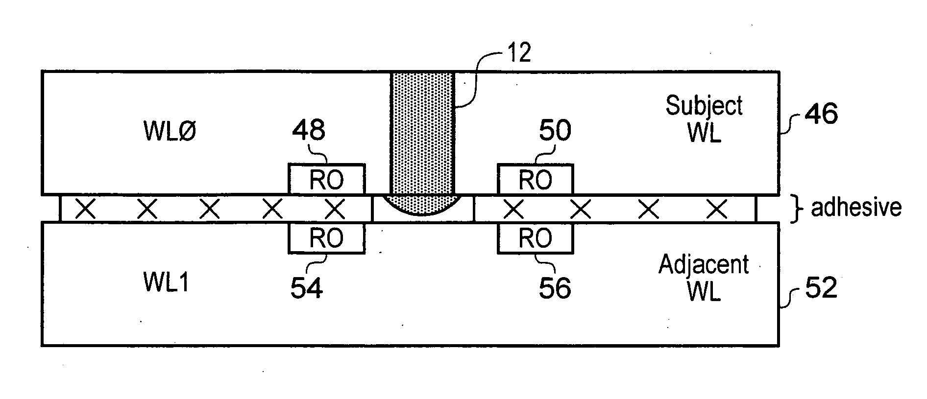
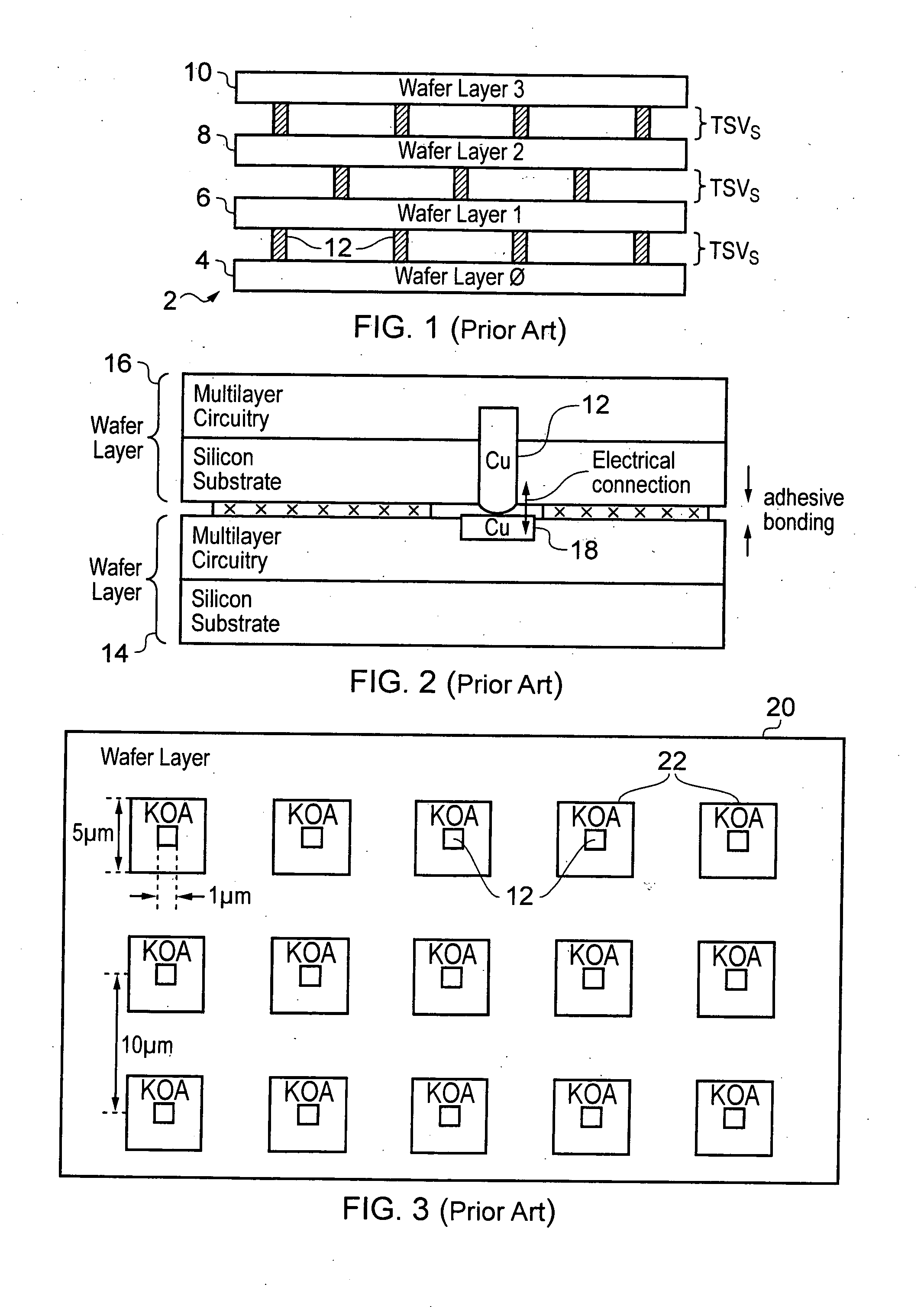
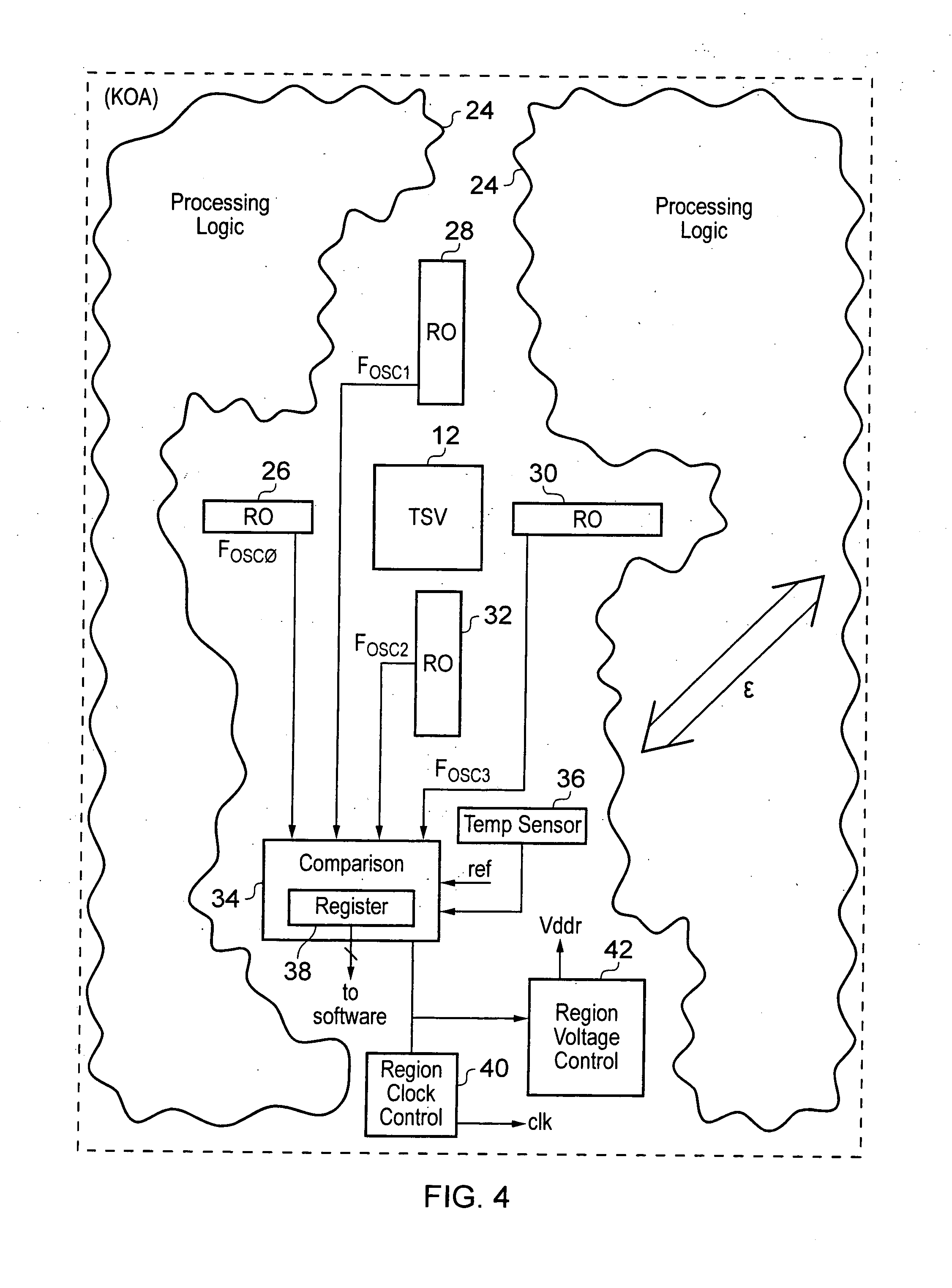
[0045]FIG. 4 schematically illustrates the region within a wafer layer of an integrated circuit surrounding a through silicon via 12. This through silicon via 12 would normally be surrounded by a keep out area KOA in which useful processing circuitry 24 would not be located as it could be subject to malfunction due electrical changes resulting from mechanical strain induced by the presence of the through silicon via 12. In accordance with the present techniques, this area proximal to the through silicon via 12 is utilised for useful processing circuitry 24. Strain sensors comprising four ring oscillators 26, 28, 30, 32, are provided surrounding the through silicon via 12. These ring oscillators 26, 28, 30, 32 are provided in pairs with each pair being disposed on an opposite side of the point at which the through silicon via 12 intersects the plane of the wafer layer. Thus, the ring oscillators 26, 28, 30, 32 can be considered as being provided in the four cardinal directions surrou...


PUM


Abstract

An integrated circuit 2 is formed of multiple wafer layers 4, 6, 8, 10 arranged in a stack and connected with through silicon vias 12. Mechanical strain sensors 26, 28, 30, 32 in the form of ring oscillators are provided proximal to the through silicon vias 12 and detect mechanical strain associated with the through silicon via 12. The measured mechanical strain may be used to dynamically adjust operating parameters of the integrated circuit either as a whole or in regions where the mechanical strain is detected. The operating parameters adjusted can include clock frequency, operating voltage and heat generation.

Description

BACKGROUND OF THE INVENTION[0001]1. Field of the Invention[0002]This invention relates to the field of integrated circuits. More particularly, this invention relates to integrated circuits formed of a stack of wafer layers interconnected by a plurality of through silicon vias.[0003]2. Description of the Prior Art[0004]FIGS. 1, 2 and 3 of the accompanying drawings schematically illustrate one example of an integrated circuit formed of a plurality of wafer layers interconnected with through silicon vias (TSVs). FIG. 1 illustrates an integrated circuit 2 comprising four wafer layers 4, 6, 8, 10 with through silicon vias 12 providing electrical connections between the wafer layers 4, 6, 8, 10. This type of technology allows more compact devices to be produced. Furthermore, the speed of communication between the wafer layers 4, 6, 8, 10 is higher than is typically achieved between separate integrated circuits each formed of one wafer layer and interconnected with a signal bus.[0005]FIG. ...

Claims


Application Information

Patent Timeline
IPC IPC(8): G01L1/00H01L23/58
CPCH01L22/12H01L22/20H01L2224/94H01L23/34H01L23/562H01L24/32H01L24/94H01L2225/06513H01L2225/06541H01L2924/01029H01L2924/14H01L2924/01033H01L2924/01074H01L2224/83
Inventor AITKEN, ROBERT CAMPBELL
Owner ARM LTD
Why Eureka
Try Eureka