Semiconductor device and method of manufacturing the semiconductor device

a semiconductor and semiconductor technology, applied in the direction of semiconductor devices, electrical appliances, transistors, etc., can solve the problems of difficult to establish a low-resistance contact between silicon and minority bits, impaired transistor uniformity, and limited minority bits in the dram, so as to achieve the effect of limiting the thickness of the gate oxide film and ensuring the uniformity of transistor characteristics

Inactive Publication Date: 2012-02-02
PS4 LUXCO SARL
View PDF3 Cites 15 Cited by
  • Summary
  • Abstract
  • Description
  • Claims
  • Application Information

AI Technical Summary

Benefits of technology

[0013]According to the method, a constricted portion is formed in the side surface of the silicon pillar by anisotropic etching, so that a particular crystal plane is dominant in the side surface of the silicon pillar. That is, the gate oxide film can be formed in a condition in which the particular crystal plane is exposed in the side surface of the silicon pillar lager than other crystal planes. In this way, variation in thickness of the gate oxide film can be limited. Therefore, the silicon pillar can be made thin without impairing the uniformity of the characteristics of the transistor.

Problems solved by technology

As a result, the occurrence of minority bits in the DRAM is limited.
However, if silicon pillar 101 is excessively thin, the area of contact with upper contact 104 is so small that it is difficult to establish a low-resistance contact between silicon pillar 101 and upper contact 104.
There is, therefore, a possibility that the uniformity of the characteristics of the transistor will be impaired.
In this way, variation in thickness of the gate oxide film can be limited.

Method used


Image

  • Semiconductor device and method of manufacturing the semiconductor device
  • Semiconductor device and method of manufacturing the semiconductor device
  • Semiconductor device and method of manufacturing the semiconductor device

Examples


Embodiment Construction

[0030]The invention will be now described herein with reference to an illustrative embodiment. Those skilled in the art will recognize that many alternative embodiments can be accomplished using the teachings of the present invention and that the invention is not limited to the embodiment illustrated for explanatory purposes.

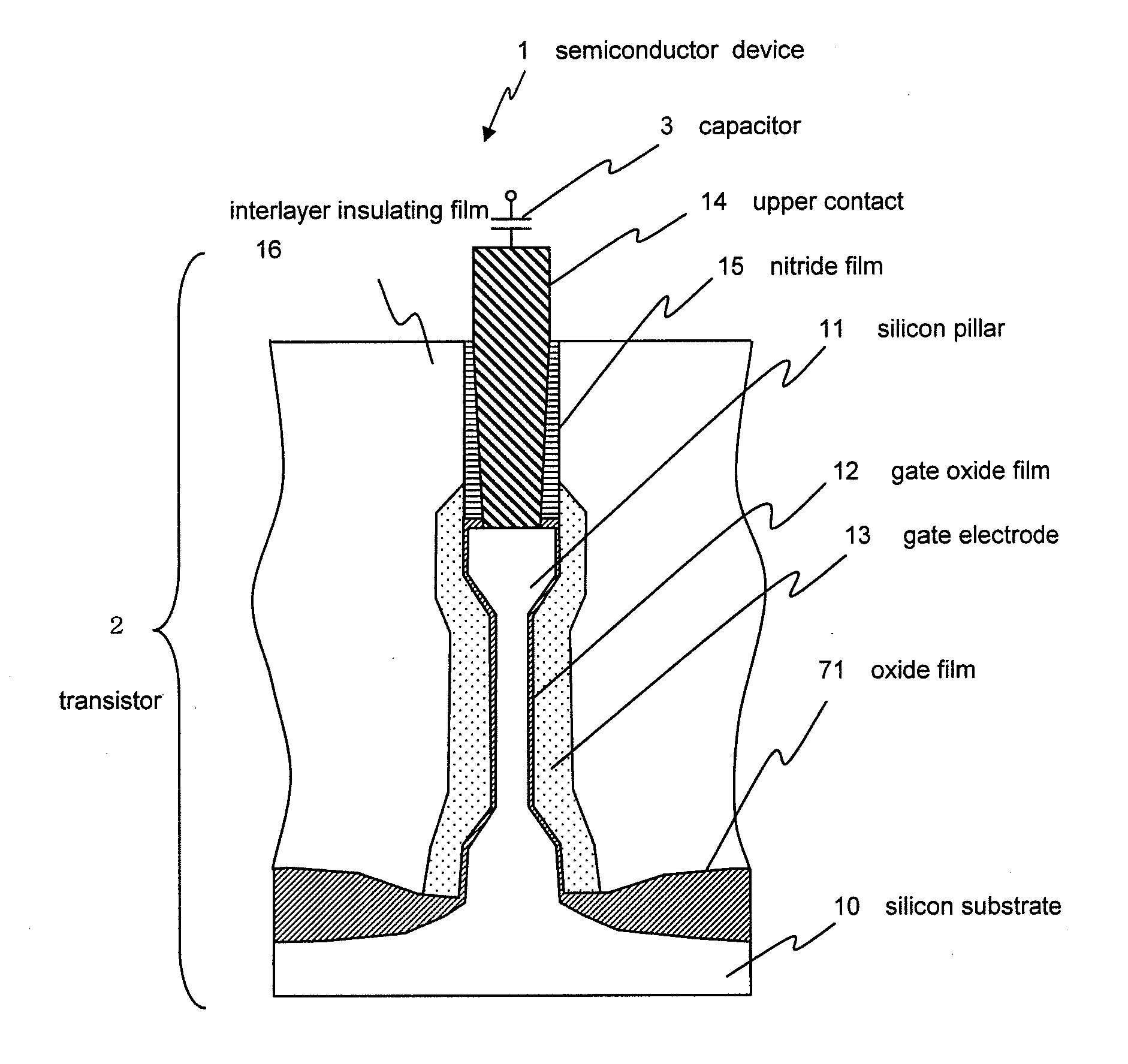
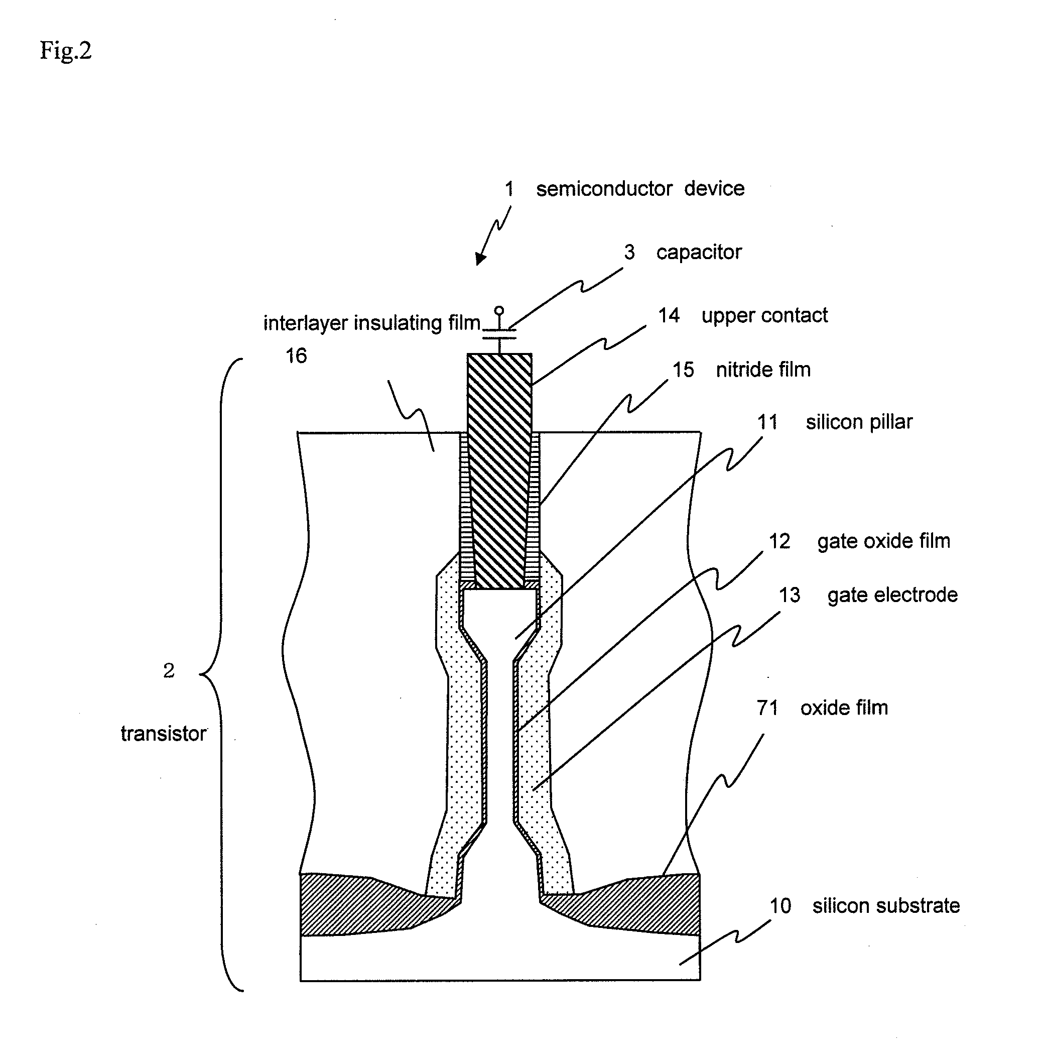
[0031]A semiconductor device in a first embodiment is a semiconductor memory which includes a capacitor and a transistor which are disposed and which are in a superposed condition and connected to each other in series. FIG. 2 is a sectional view showing the structure of a main portion of the semiconductor device in the exemplary embodiment.

[0032]Semiconductor device 1 of the exemplary embodiment has, as shown in FIG. 2, transistor 2 and capacitor 3 disposed by being superposed on transistor 2 and connected to transistor 2 in series. In transistor 2, when a voltage is applied to gate electrode 13, a channel is produced in silicon pillar 11, and a longitudinal cur...


PUM


Abstract

A method of manufacturing a semiconductor device includes forming silicon pillar 11 on substrate 10, forming a protective film which covers an upper end portion and a lower end portion of a side surface of silicon pillar 11, forming a constricted portion by anisotropic etching in a portion of the side surface of silicon pillar 11 which is not covered with the protective film after forming the protective film, removing the protective film after forming the constricted portion, forming gate oxide film 12 which covers the side surface of silicon pillar 11 in which the constricted portion is formed, and forming gate electrode 13 which covers gate oxide film 12.

Description

CROSS-REFERENCE TO RELATED APPLICATION[0001]This application is a divisional of U.S. patent application Ser. No. 12 / 633,332 filed Dec. 8, 2009, which is based upon and claims the benefit of priority from Japanese Patent Application No. 2008-313363 filed on Dec. 9, 2008, the contents of all of which are incorporated herein by reference in their entirety.BACKGROUND OF THE INVENTION[0002]1. Field of the Invention[0003]The present invention relates to a semiconductor device comprising a silicon pillar formed on a substrate and to a method of manufacturing the semiconductor device.[0004]2. Description of Related Art[0005]With respect to semiconductor memories as one kind of semiconductor device, there has been a demand for reducing the chip area year by year for the purpose of achieving a low cost. To meet this demand, 4F2 (2F×2F) cell structures have been proposed for dynamic random access memories (DRAMs) which is one kind of semiconductor memory. “4F2” means the area of a memory cell ...

Claims


Application Information

Patent Timeline
Patent Type & Authority Applications(United States)
IPC IPC(8): H01L27/06
CPCH01L27/10823H01L27/10876H01L29/7827H01L29/66666H01L29/0657H10B12/34H10B12/053
Inventor NOJIMA, KAZUHIRO
Owner PS4 LUXCO SARL
Why Eureka
Try Eureka