Antiphase Domain Boundary-Free III-V Compound Semiconductor Material on Semiconductor Substrate and Method for Manufacturing Thereof

a compound semiconductor material and antiphase domain technology, applied in the direction of semiconductor devices, basic electric elements, electrical apparatus, etc., can solve the problems of large lattice-mismatch between the lattice constant of iii-v materials and the lattice constant of silicon, the difficulty of epitaxial growth defect-free iii-v materials, and the deterioration of the electrical performance of the devi

a compound semiconductor material and antiphase domain technology, applied in the direction of semiconductor devices, basic electric elements, electrical apparatus, etc., can solve the problems of large lattice-mismatch between the lattice constant of iii-v materials and the lattice constant of silicon, the difficulty of epitaxial growth defect-free iii-v materials, and the deterioration of the electrical performance of the devi

US20120032234A1Active Publication Date: 2012-02-09INTERUNIVERSITAIR MICRO ELECTRONICS CENT (IMEC VZW) +1

Image

  • Antiphase Domain Boundary-Free III-V Compound Semiconductor Material on Semiconductor Substrate and Method for Manufacturing Thereof
  • Antiphase Domain Boundary-Free III-V Compound Semiconductor Material on Semiconductor Substrate and Method for Manufacturing Thereof
  • Antiphase Domain Boundary-Free III-V Compound Semiconductor Material on Semiconductor Substrate and Method for Manufacturing Thereof

Examples


Embodiment Construction

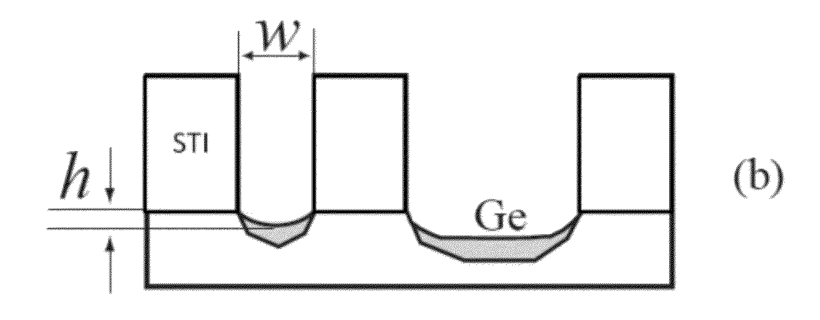
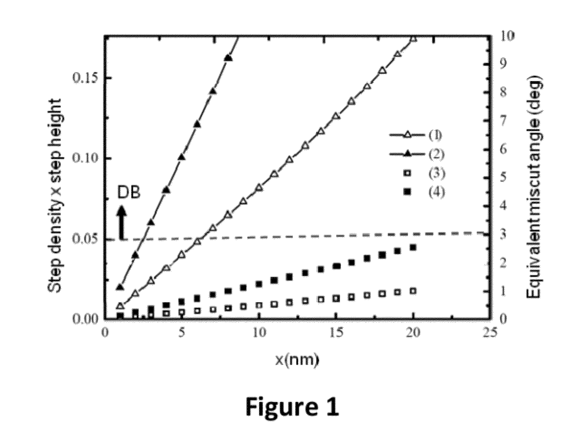
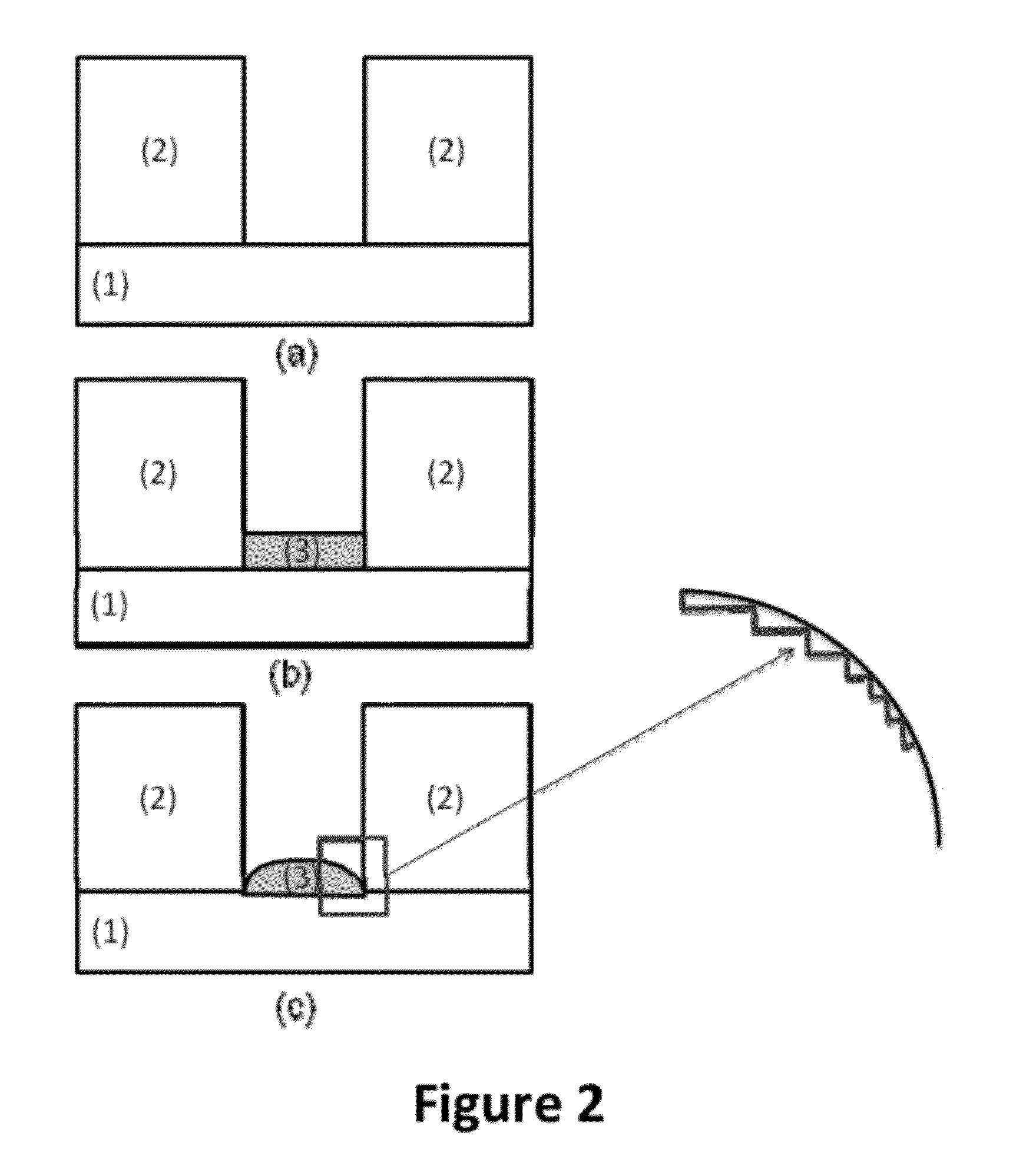
[0021]The present invention will be described with respect to particular embodiments and with reference to certain drawings but the invention is not limited thereto but only by the claims. The drawings described are only schematic and are non-limiting. In the drawings, the size of some of the elements may be exaggerated and not drawn on scale for illustrative purposes. The dimensions and the relative dimensions do not necessarily correspond to actual reductions to practice of the invention.

[0022]Furthermore, the terms first, second, third and the like in the description and in the claims, are used for distinguishing between similar elements and not necessarily for describing a sequential or chronological order. The terms are interchangeable under appropriate circumstances and the embodiments of the invention can operate in other sequences than described or illustrated herein.

[0023]Moreover, the terms top, bottom, over, under and the like in the description and the claims are used fo...


PUM


Abstract

Methods of manufacturing a III-V compound semiconductor material, and the semiconductor material thus manufactured, are disclosed. In one embodiment, the method comprises providing a substrate comprising a first semiconductor material having a {001} orientation and an insulating layer overlaying the first semiconductor material. The insulating layer comprises a recessed region exposing an exposed region of the first semiconductor material. The method further comprises forming a buffer layer overlaying the exposed region that comprises a group IV semiconductor material. The method further comprises thermally annealing the substrate and the buffer layer, thereby roughening the buffer layer to create a rounded, double-stepped surface having a step density and a step height. A product of the step density and the step height is greater than or equal to 0.05 on the surface. The method further comprises at least partially filling the recessed region with a III-V compound semiconductor material overlaying the surface.

Description

CROSS-REFERENCE TO RELATED APPLICATIONS[0001]The present application is a non-provisional of U.S. Provisional Patent Application Ser. No. 61 / 371,008 filed Aug. 5, 2010, the contents of which are hereby incorporated by reference.BACKGROUND[0002]The present invention relates to an engineered substrate comprising a III-V compound semiconductor material thereon and a method for manufacturing such a III-V compound semiconductor material on a semiconductor substrate.[0003]Development of high performance III-V complementary metal-oxide-semiconductor (CMOS) devices, a type of CMOS utilizing high mobility III-V materials (such as gallium arsenide or indium gallium arsenide as channels instead of silicon, has been suffering from the difficulties of epitaxially growing defect-free III-V materials on silicon substrates.[0004]One difficulty of epitaxially growing III-V materials on silicon substrates is that there is a large lattice-mismatch between the lattice constants of III-V materials and t...

Claims


Application Information

Patent Timeline
09 Feb 2012
Publication
US20120032234A1
IPC
H01L21/20; H01L29/267
CPC
H01L21/02381; H01L21/0245; H01L21/02461; H01L21/02463; H01L21/02639; H01L21/02538; H01L21/02543; H01L21/02546
Inventors
WANG, GANG; CAYMAX, MATTY