CMOS transistors with stressed high mobility channels

a technology of high-mobility channels and transistors, applied in the field of complementary metaloxidesemiconductor (cmos) field effect transistors, to achieve the effect of enhancing the mobility of charge carriers

Inactive Publication Date: 2012-02-16
ALSEPHINA INNOVATIONS INC
View PDF1 Cites 46 Cited by
  • Summary
  • Abstract
  • Description
  • Claims
  • Application Information

AI Technical Summary

Benefits of technology

[0006]In one embodiment, a p-type field effect transistor (PFET) and an n-type field effect transistor (NFET) are formed in a silicon-germanium alloy layer. Source and drain regions of the PFET are formed employing embedded germanium-containing regions, and source and drain regions of the NFET are formed employing embedded silicon-containing regions. The embedded germanium-containing regions apply a compressive stress to the channel of the PFET, and the embedded silicon-containing regions apply a tensile stress to the channel of the NFET. The compressive stress and the tensile stress enhance the mobility of charge carriers in the PFET and the NFET, respectively.
[0007]In another embodiment, a p-type field effect transistor (PFET) and an n-type field effect transistor (NFET) are formed in a germanium layer. Source and drain regions of the PFET are formed by implanting a Group IIIA element having an atomic radius greater than the atomic radius of germanium into portions of the germanium layer, and source and drain regions of the NFET are formed employing embedded silicon-germanium alloy regions. The Group IIIA element-containing source and drain regions apply a compressive stress to the channel of the PFET, and the embedded silicon-germanium alloy regions apply a tensile stress to the channel of the NFET. The compressive stress and the tensile stress enhance the mobility of charge carriers in the PFET and the NFET, respectively.

Problems solved by technology

While such beneficial effects of stress are known in the art, a difficulty arises since two different types of field effect transistors require two different types of stress.

Method used


Image

  • CMOS transistors with stressed high mobility channels
  • CMOS transistors with stressed high mobility channels
  • CMOS transistors with stressed high mobility channels

Examples


first embodiment

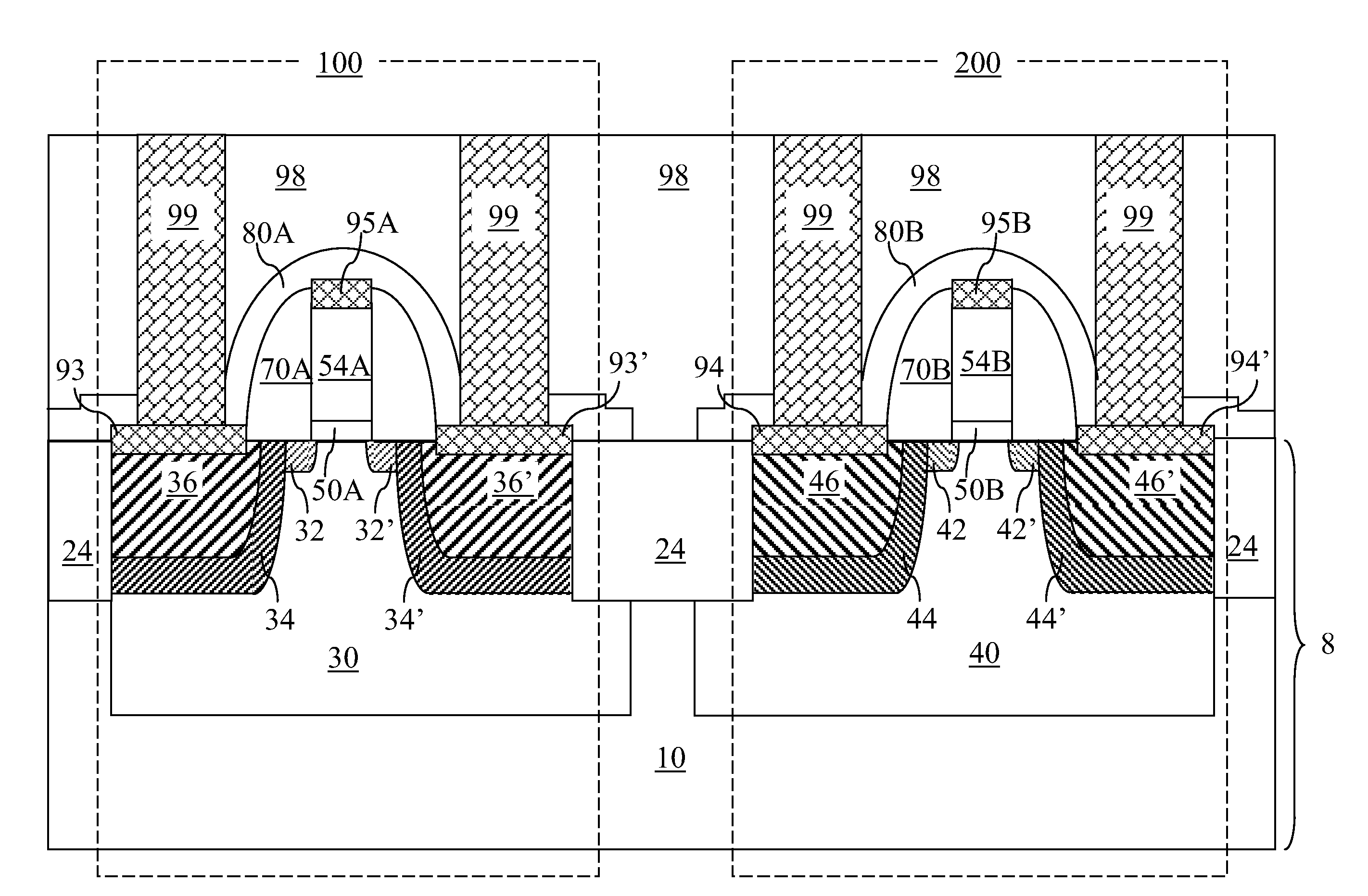
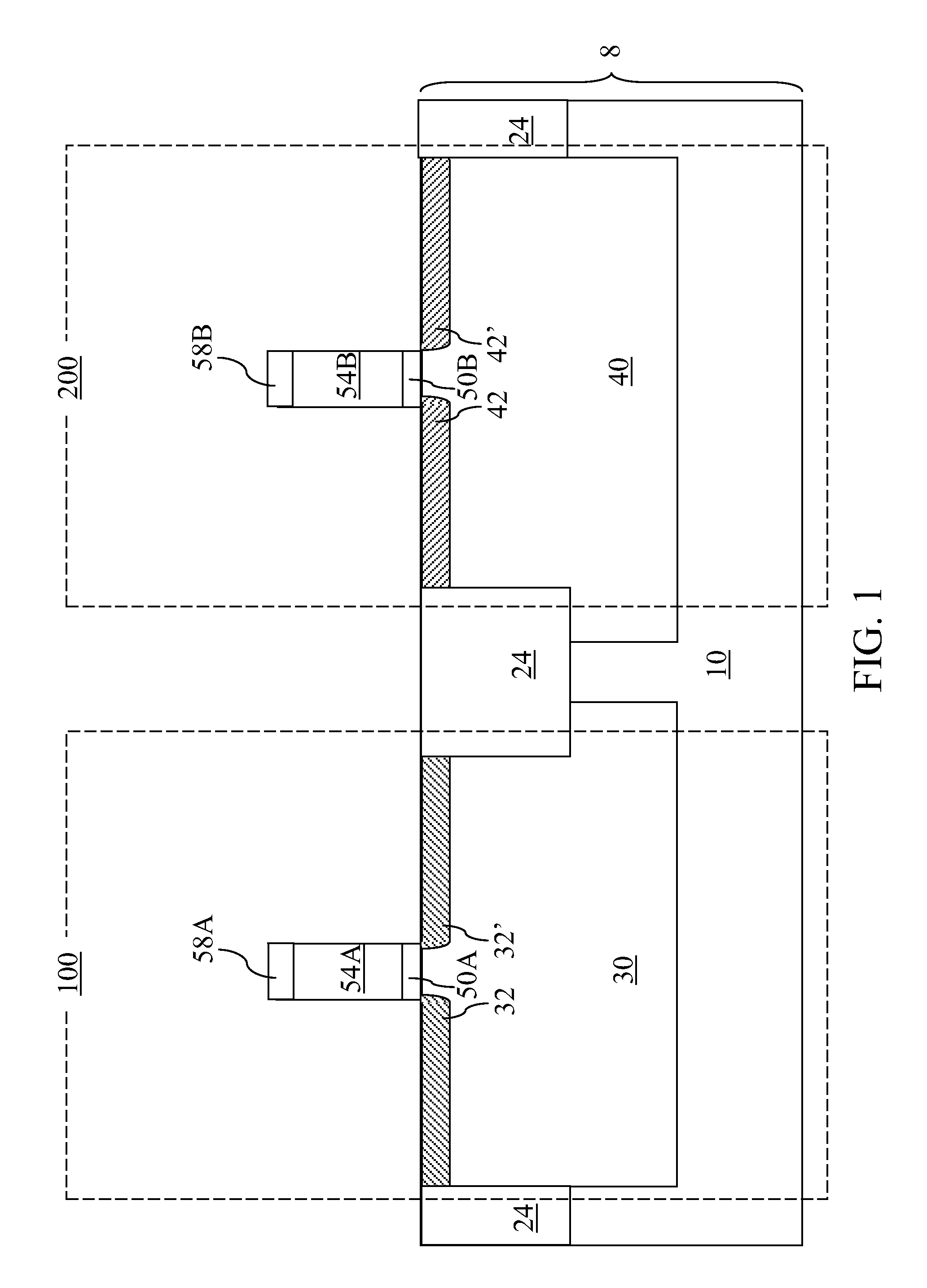
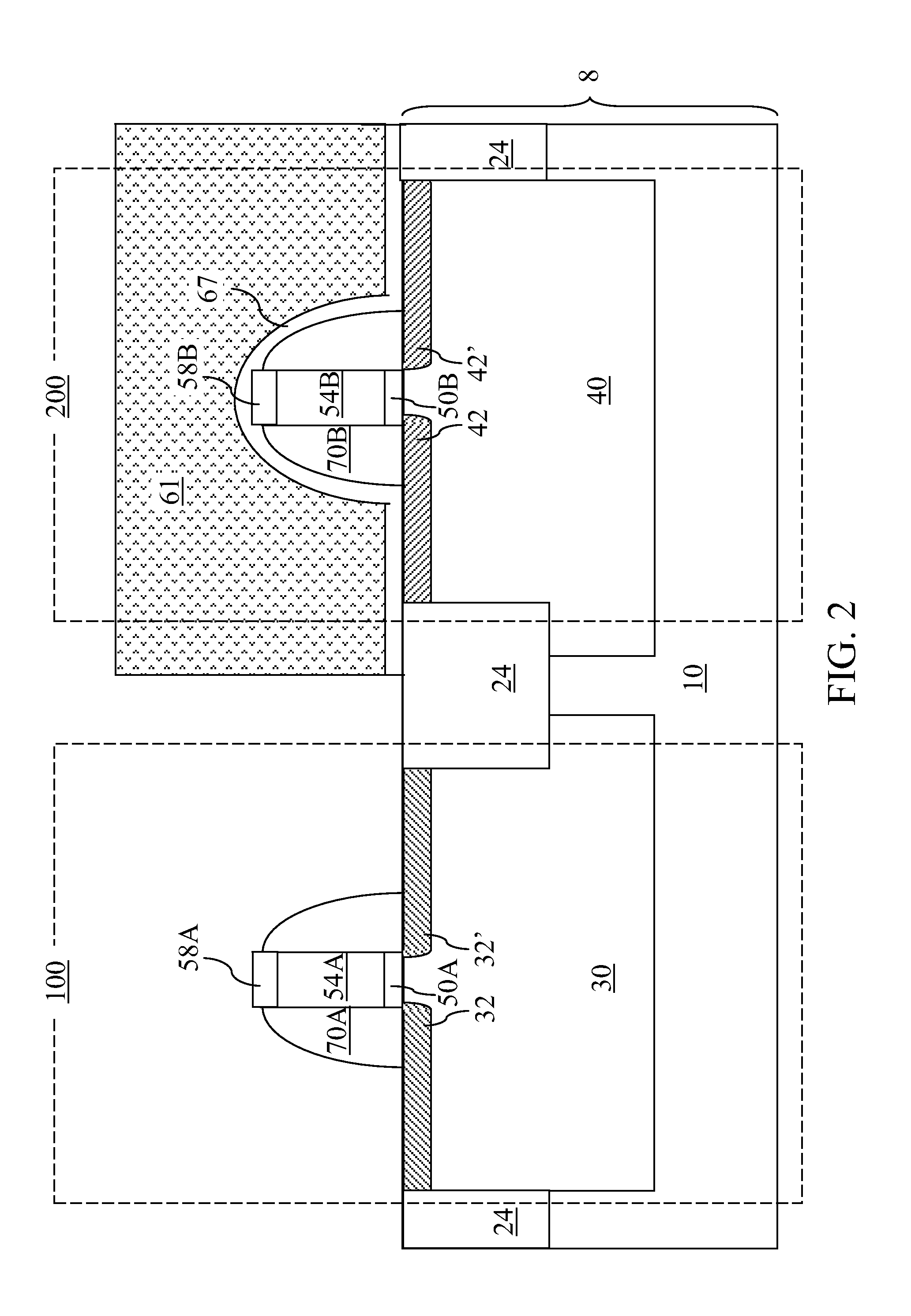
[0027]Referring to FIG. 1, a first exemplary semiconductor structure according to the present disclosure includes a substrate 8. The substrate 8 includes a silicon-germanium alloy layer, which can include an underlying silicon-germanium alloy layer 10, a p-doped silicon-germanium alloy region 30 that is an n-doped portion of the silicon-germanium alloy layer, and an n-doped silicon-germanium alloy region 40 that is a p-doped portion of the silicon-germanium alloy layer. The p-doped silicon-germanium alloy region 30 can function as a p-type well, and the n-doped silicon-germanium alloy region 40 can function as an n-type well. The underlying silicon-germanium alloy layer 10 may be intrinsic, p-doped, or n-doped. The silicon-germanium alloy layer (10, 30, 40) can have an atomic germanium concentration from 1.0% to 99.0%, and typically from 10% to 90%, and more typically from 25% to 75%. The silicon-to-germanium ratio is constant throughout the silicon-germanium alloy layer (10, 30, 40...

second embodiment

[0090]Referring to FIG. 15, a second exemplary semiconductor structure according to the present disclosure includes a substrate 8′. The substrate 8′ includes a germanium layer, which can include an underlying germanium layer 110, a p-doped germanium region 130 that is an n-doped portion of the germanium layer, and an n-doped germanium region 140 that is a p-doped portion of the germanium layer. The p-doped germanium region 130 can function as a p-type well, and the n-doped germanium region 140 can function as an n-type well. The underlying germanium layer 10 may be intrinsic, p-doped, or n-doped. The germanium layer (110, 130, 140) can consist of germanium if undoped, or can consist of germanium and p-type or n-type dopants.

[0091]The substrate 8′ may be a bulk substrate including the germanium layer (110, 130, 140) at the top portion thereof. Alternately, the substrate 8′ can be a semiconductor-on-insulator (SOI) substrate that includes a buried insulator layer (not shown). In this ...


PUM


Abstract

A p-type field effect transistor (PFET) having a compressively stressed channel and an n-type field effect transistor (NFET) having a tensilely stressed channel are formed. In one embodiment, a silicon-germanium alloy is employed as a device layer, and the source and drain regions of the PFET are formed employing embedded germanium-containing regions, and source and drain regions of the NFET are formed employing embedded silicon-containing regions. In another embodiment, a germanium layer is employed as a device layer, and the source and drain regions of the PFET are formed by implanting a Group IIIA element having an atomic radius greater than the atomic radius of germanium into portions of the germanium layer, and source and drain regions of the NFET are formed employing embedded silicon-germanium alloy regions. The compressive stress and the tensile stress enhance the mobility of charge carriers in the PFET and the NFET, respectively.

Description

BACKGROUND[0001]The present disclosure generally relates to semiconductor devices, and particularly to complementary metal-oxide-semiconductor (CMOS) field effect transistors including a p-type field effect transistor (PFET) having a compressively stressed channel and an n-type field effect transistor (NFET) having a tensilely stressed channel, and methods of manufacturing the same.[0002]Carrier mobility in a metal oxide semiconductor field effect transistor (MOSFET) may be manipulated by a stress applied to the channel of the MOSFET. Even relatively small changes in the stress of the channel may result in large changes in carrier mobility for some combinations of semiconductor material and crystallographic orientations, and may be utilized to increase the transconductance (or reduced serial resistance) of the MOSFET, thereby enhancing the performance of the MOSFET.[0003]When stress is applied to the channel of a semiconductor transistor, the applied stress and the resulting strain ...

Claims


Application Information

Patent Timeline
Patent Type & Authority Applications(United States)
IPC IPC(8): H01L27/092H01L21/20
CPCH01L21/823807H01L21/823814H01L29/7843H01L29/7848
Inventor BEDELL, STEPHEN W.KIM, JEE H.MAURER, SIEGFRIED L.REZNICEK, ALEXANDERSADANA, DEVENDRA K.
Owner ALSEPHINA INNOVATIONS INC
Why Eureka
Try Eureka