Light emitting element

a technology light sources, applied in the field can solve the problems of limited enhancement of achieve the effect of enhancing the light extraction efficiency of light emitting elements

Active Publication Date: 2012-03-01
TOYODA GOSEI CO LTD
View PDF0 Cites 86 Cited by
  • Summary
  • Abstract
  • Description
  • Claims
  • Application Information

AI Technical Summary

Benefits of technology

[0026]According to one embodiment of the invention. a light emitting element is constructed such that a contact electrode on a p-side contact layer of a p-type semiconductor layer is formed of ITO transparent to light emitted from an active layer thereof, a first reflecting layer is formed thereon, and a second reflecting layer is formed on a p-side first insulat

Problems solved by technology

Therefore. the light emitting element is limited

Method used


Image

  • Light emitting element
  • Light emitting element
  • Light emitting element

Examples


first embodiment

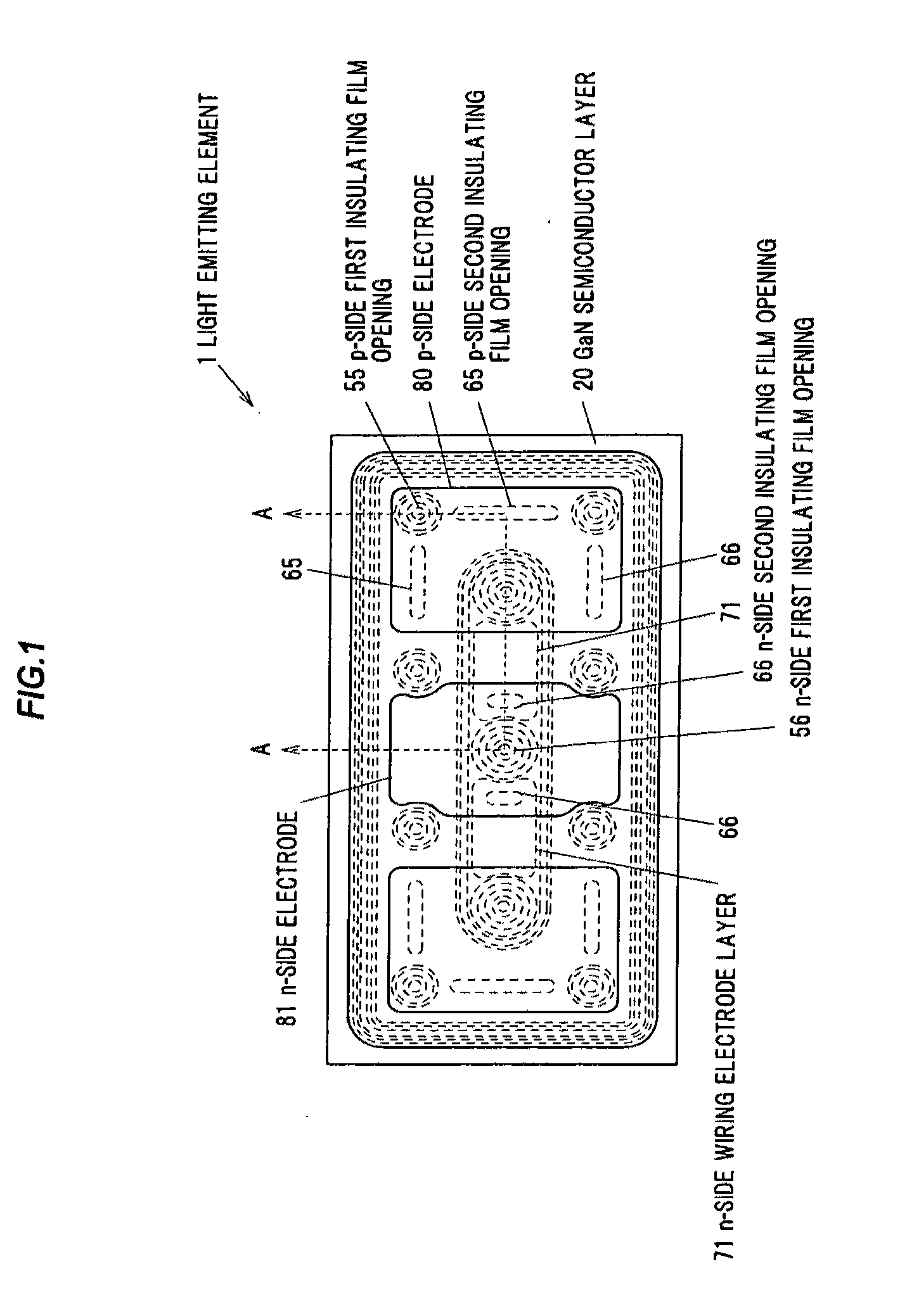
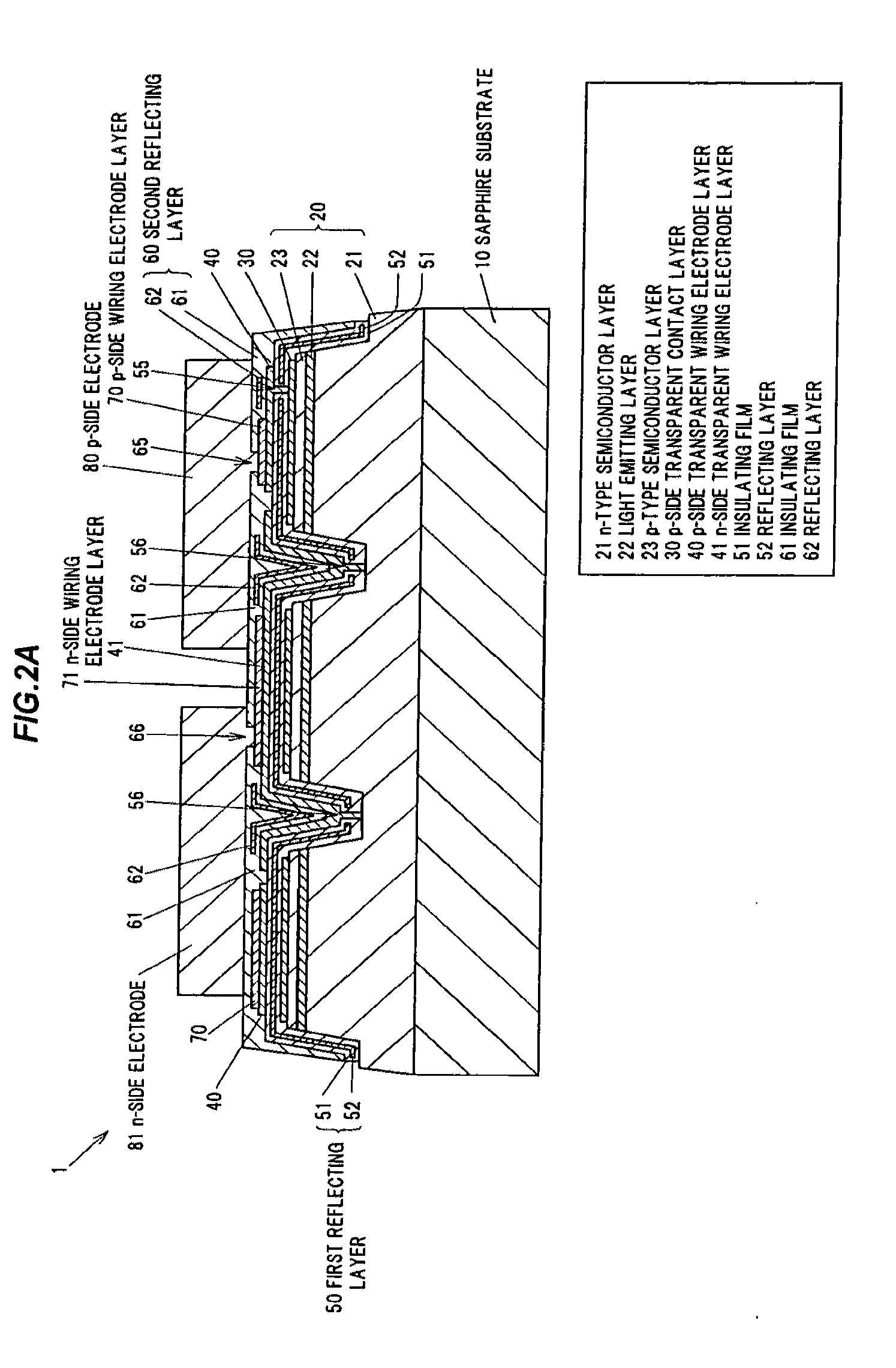
[0034]Structure of Light Emitting Element 1

[0035]FIG. 1 is a plan view schematically showing a structure of a light emitting element according to a first embodiment of the present invention.FIG. 2A is a cross-sectional view taken along the line A-A in FIG. 1 and FIG. 2B is a partial enlarged view of FIG. 2A.

[0036]As shown in FIG. 1. the light emitting element 1 according to the first embodiment of the present invention is of a flip-chip type one and is formed so as to have a rectangular shape in a plan view. In addition, as shown in FIG. 2A. the light emitting element 1 includes a sapphire substrate 10 having a c-plane (0001). and a GaN semiconductor layer 20 formed on the sapphire substrate 10. The GaN semiconductor layer 20 has a buffer layer (not shown), an n-type semiconductor layer 21 formed on the buffer layer. a light emitting layer 22 formed on the n-type semiconductor layer 21 and a, p-type semiconductor layer 23 formed on the light emitting layer 22 in this order from the ...

second embodiment

[0076]FIG. 4 is a plan view schematically showing a structure of a light emitting element 1A according to a second embodiment of the present invention.

[0077]The light emitting element 1A has a structure that the p-side transparent contact electrode 30 of the light emitting element 1 according to the first embodiment is changed to the p-side contact electrode 32 including a high reflective material such as Ag, Rh being not transparent, and an insulating film 53 that does not have a reflective layer is formed instead of the first reflecting layer 50 of the first embodiment. Namely, in the light emitting element 1A, the p-side contact electrode 32 functions as the first reflecting layer.

[0078]In addition, a region in which a part of the n-type semiconductor layer 21 is exposed functions as the openings.

[0079]Operation

[0080]The light emitting element 1A emits a light from the light emitting layer 22 by applying voltage to the p-side electrode 80 and the n-side electrode 81. A part of th...

third embodiment

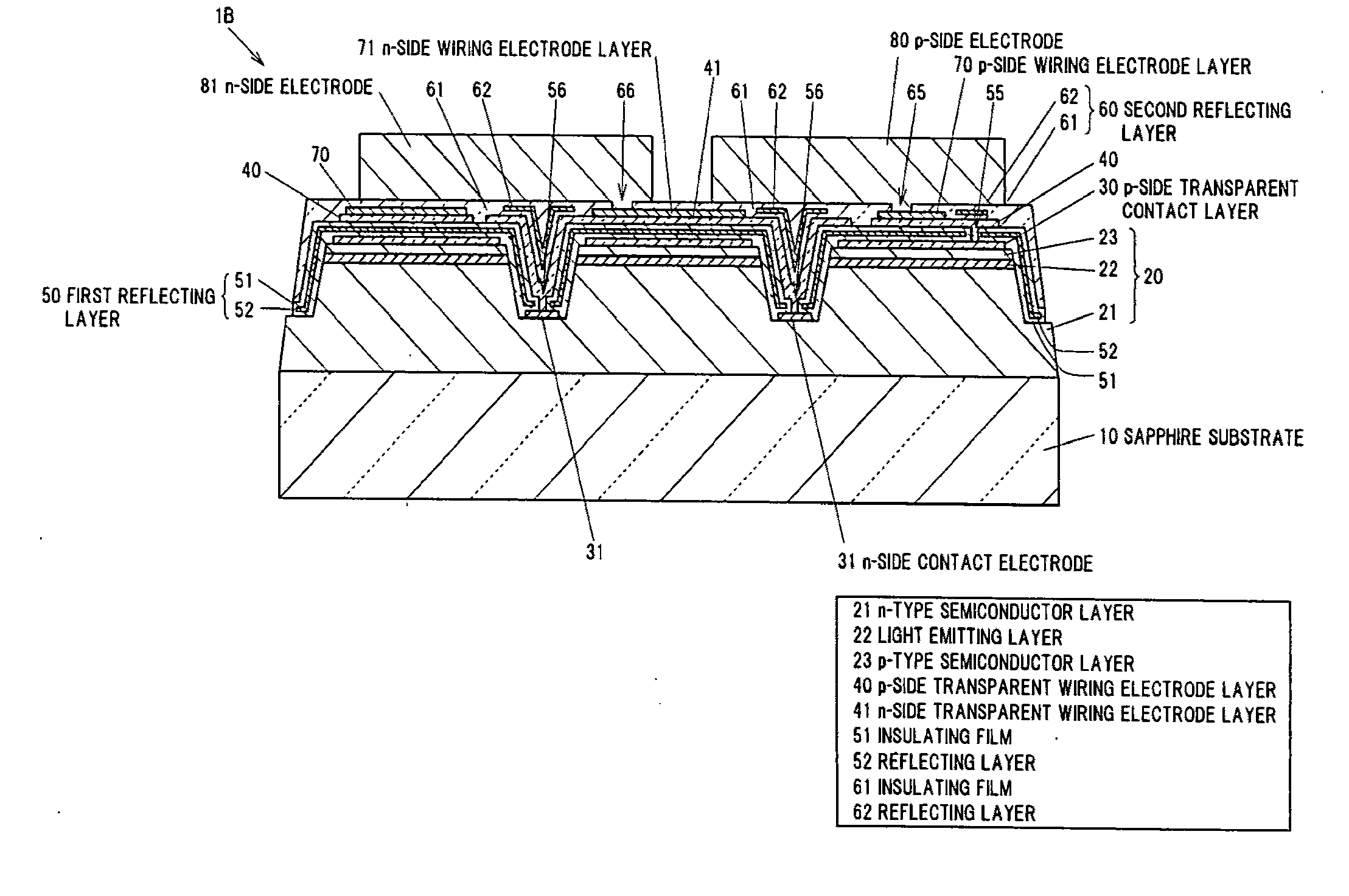
[0084]FIG. 5 is a plan view schematically showing a structure of a light emitting element 1B according to a third embodiment of the present invention.

[0085]The light emitting element 1B differs from the light emitting element 1 according to the first embodiment in having a structure that the n-side contact electrode 31 is formed between the n-side contact layer of the n-type semiconductor layer 21 and the n-side transparent wiring electrode layer 41. The n-side contact electrode 31 is formed of a material having conductive property and translucency to a wavelength of a light emitted from the light emitting layer 22, and is formed of the same electrode material as that of the n-side transparent wiring electrode layer 41. The n-side contact electrode 31 is formed of, for example, ITO.

[0086]As shown in FIG. 5, one surface of the n-side contact electrode 31 comes into contact with the n-side transparent wiring electrode layer 41, and another surface comes into contact with the n-type se...


PUM


Abstract

A light emitting element includes a semiconductor laminate structure including a first semiconductor layer of a first conductivity type, a light emitting layer, and a second semiconductor layer of a second conductivity type different from the first conductivity type, a part of the second semiconductor layer and the light emitting layer being removed to expose a part of the first semiconductor layer: a first reflecting layer on the semiconductor laminate structure and including an opening, the opening being formed in the exposed part of the first semiconductor layer, a transparent wiring electrode for carrier injection into the first semiconductor layer or the second semiconductor layer through the opening, a second reflecting layer formed on the transparent wiring electrode and covering a part of the opening so as to reflect light emitted from the light emitting layer and passing through the opening back to the first semiconductor layer.

Description

[0001]The present application is based on Japanese patent application Nos.2010-190779 and 2011-128390 tiled on Aug. 27, 2010 and June 8, 2011. respectively, the entire contents of which are incorporated herein by reference.BACKGROUND OF THE INVENTION[0002]1. FIELD OF THE INVENTION[0003]This invention relates to a light emitting element with a structure to reflect light emitted therein in a light extracting direction thereof[0004]2. DESCRIPTION OF THE RELATED ART[0005]Heretofore, a light emitting element of a Clip-chip type in which a p-type electrode and an n-type electrode are formed in the same surface of a nitride semiconductor formed on a sapphire substrate is known (for example. JP-A-2008-288548). The light emitting element disclosed in JP-A-2008-288548 has a light emitting layer between a p-type semiconductor layer and an n-type semiconductor layer, and a diffusion electrode having translucency composed of Indium Tin Oxide (ITO) or the like is formed on the p-type semiconducto...

Claims


Application Information

Patent Timeline
IPC IPC(8): H01L33/60
CPCH01L33/382H01L33/46H01L2933/0025H01L33/42H01L2924/0002H01L33/60H01L2924/00H01L33/20
Inventor KAMIYA, MASAODEGUCHI, MASASHI
Owner TOYODA GOSEI CO LTD
Why Eureka
Try Eureka