Package structure having through-silicon-via (TSV) chip embedded therein and fabrication method thereof

a technology of throughsiliconvia and packaging structure, which is applied in the direction of semiconductor devices, semiconductor/solid-state device details, electrical apparatus, etc., can solve the problems of inability to achieve satisfactory electron products, inability to effectively reduce the spacing between the electrode pads b>120, and inability to meet the requirements of the electron product. achieve the effect of high wiring density semiconductor chips

Inactive Publication Date: 2012-03-01
UNIMICRON TECH CORP
View PDF7 Cites 43 Cited by
  • Summary
  • Abstract
  • Description
  • Claims
  • Application Information

AI Technical Summary

Benefits of technology

[0020]In summary, the package structure having an embedded TSV chip and the fabrication method of the present invention are based on the embedded TSV chip enabling the package structure to have the electrical connection pads (the electrode pads of the TSV chip) for the corresponding high wiring density chip (the first chip). Therefore, the purpose of integrating high wiring density semiconductor chips can be achieved.

Problems solved by technology

However, the spacing between the electrical contact pads 100 of the package substrate 10 is based on a micrometer in length per unit, and cannot be effectively reduced to the spacing between the electrode pads 120.
Although the semiconductor chip 12 has a high wiring density, no compatible package substrates are available.
As a result, the electron products cannot be satisfactorily realized.

Method used


Image

  • Package structure having through-silicon-via (TSV) chip embedded therein and fabrication method thereof
  • Package structure having through-silicon-via (TSV) chip embedded therein and fabrication method thereof
  • Package structure having through-silicon-via (TSV) chip embedded therein and fabrication method thereof

Examples


Embodiment Construction

[0023]The following embodiments are provided to illustrate the disclosure of the present invention. These and other advantages and effects can be apparent to one ordinarily skilled in the art after reading the disclosure of this specification.

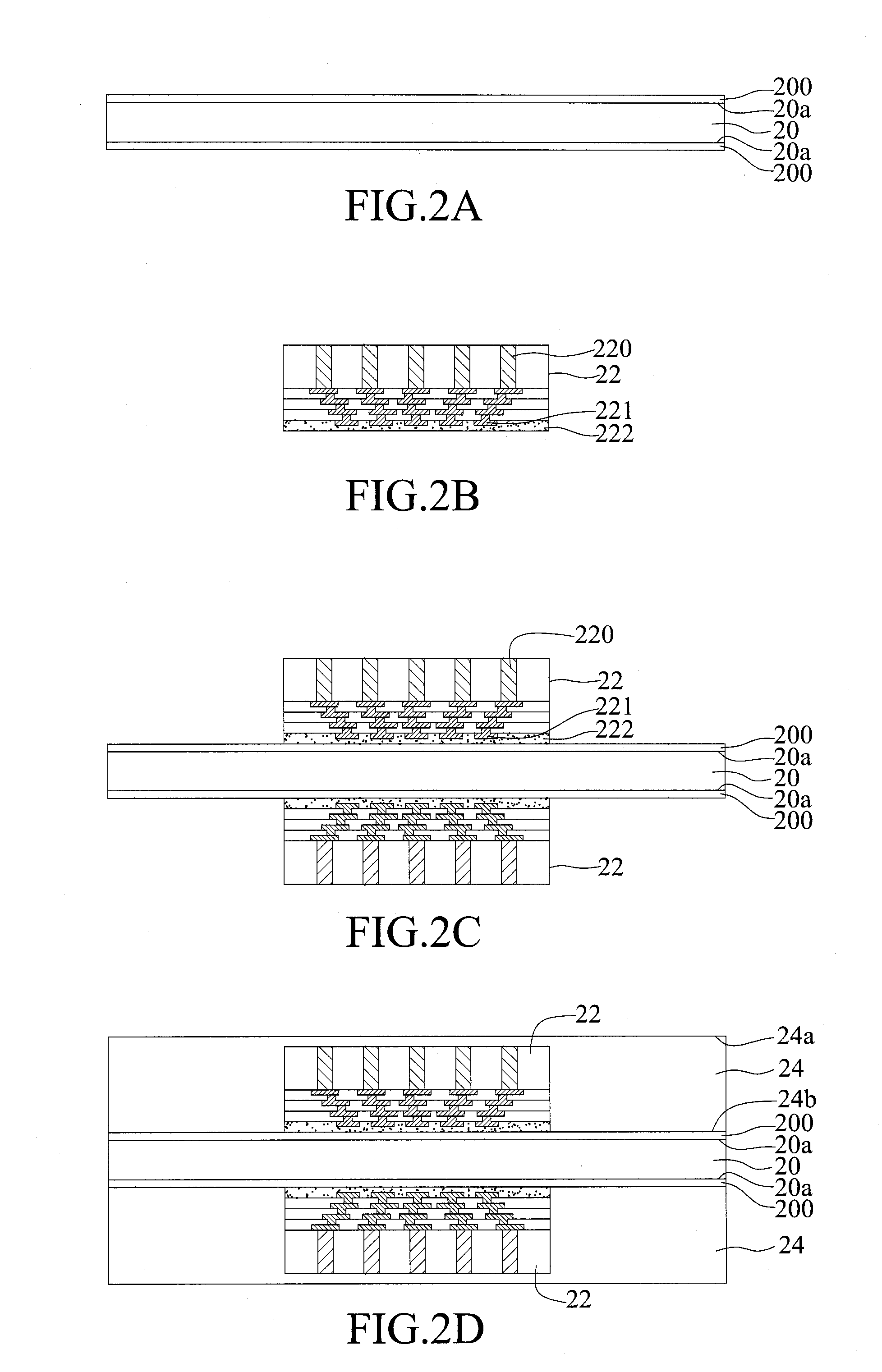
[0024]FIGS. 2A to 2I are schematic cross-sectional views illustrating a fabrication method for the package structure having an embedded TSV chip according to the present invention.

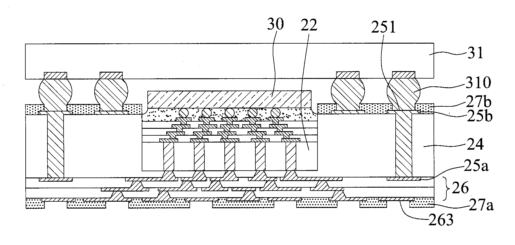
[0025]As shown in FIGS. 2A and 2B, a carrier board 20 and a TSV chip 22 having a plurality of conductive TSVs 220 are provided. Both surfaces 20a of the carrier board 20 are each covered by a release film 200, respectively.

[0026]The TSV chip 22, for example, can be a silicon TSV chip. The conductive TSVs 220 are electrically connected to electrode pads 221. Furthermore, the spacing between any two of the electrode pads 221 is based on a nanometer in length per unit, and the electrode pads 221 are coated by a protective layer 222.

[0027]As shown in FIG. 2C, the protecti...


PUM


Abstract

A package structure includes a dielectric layer having a first surface and a second surface; a through-silicon-via (TSV) chip embedded in the dielectric layer, wherein the TSV chip has a plurality of conductive TSVs, and electrode pads formed on a surface of the TSV chip that are electrically connected to the conductive TSVs and exposed from the second surface of the dielectric layer; and a first circuit layer formed on the first surface of the dielectric layer, wherein the first circuit layer is connected to the conductive TSVs of the TSV chip by the conductive blind vias, so that the high wiring density semiconductor chip can be disposed on the electrode pads of the TSV chip in order to integrate high wiring density semiconductor chips. The invention also provides a fabrication method for fabricating the package structure having an embedded TSV chip.

Description

BACKGROUND OF THE INVENTION[0001]1. Field of the Invention[0002]The present invention relates to package structures and fabrication methods thereof, and more particularly, to a package structure having an embedded through-silicon-via (TSV) chip and a fabrication method thereof.[0003]2. Description of Related Art[0004]With the vigorous development of electronic industry, the size of electronic products is trending small and the trend of their functions is towards the Research and Development (R&D) direction of high performance, high functionality, and high speed. In order to satisfy the demand of semiconductor devices with high integration and miniaturization, not only the semiconductor packaging technology of the conventional wire bonding method but also the flip chip method can be used to enhance the wiring density. FIG. 1 shows a schematic cross-sectional view of the conventional flip chip package structure.[0005]Referring to FIG. 1, the package structure includes a package substr...

Claims


Application Information

Patent Timeline
Patent Type & Authority Applications(United States)
IPC IPC(8): H01L23/48H01L21/50
CPCH01L21/486H01L21/568H01L21/6835H01L23/13H01L23/147H01L23/3121H01L23/49827H01L23/49833H01L25/03H01L2224/16227H01L2224/32145H01L2224/48091H01L2224/48227H01L2224/73204H01L2224/73265H01L2225/06513H01L2225/06541H01L2225/06548H01L2924/10253H01L2924/15174H01L2924/15184H01L24/48H01L2924/01033H01L2924/014H01L25/105H01L2225/0651H01L2225/1035H01L2225/1058H01L2225/06558H01L2224/04105H01L2924/15321H01L2924/1533H01L24/05H01L24/16H01L24/19H01L24/20H01L24/32H01L24/73H01L2224/05025H01L2224/16145H01L2224/73259H01L2224/16225H01L2224/32225H01L2924/15311H01L2224/27013H01L2224/0401H01L2924/00014H01L2924/00012H01L2924/00011H01L2924/00015H01L2924/00H01L2924/181H01L2224/45099H01L2224/45015H01L2924/207
Inventor ZENG, ZHAO-CHONG
Owner UNIMICRON TECH CORP
Why Eureka
Try Eureka