Semiconductor device including latch circuit

a latch circuit and semiconductor technology, applied in logic circuits, logic functions, pulse techniques, etc., can solve the problems of data retention deterioration due to the increase in the number of rewrite operations, and achieve the effect of suppressing data retention deterioration and reducing the number of transistors

Inactive Publication Date: 2012-03-01
SEMICON ENERGY LAB CO LTD
View PDF5 Cites 22 Cited by
  • Summary
  • Abstract
  • Description
  • Claims
  • Application Information

AI Technical Summary

Benefits of technology

[0017]In the latch circuit according to one embodiment of the present invention, data is stored in a node that is electrically connected to one of a source and a drain of a transistor whose channel region is formed with an oxide semiconductor and is brought into a floating state when the transistor is turned off. Note that the off-state current (leakage current) of the transistor is extremely low. Therefore, when the potential of the node is set to a specific value and then the transistor is turned off, the potential can be kept constant or almost constant. Consequently, data can be accurately retained in the latch circuit. Furthermore, the transistor is kept off even when supply of power to the latch circuit is stopped. As a result, data can be retained in the latch circuit even when power supply is stopped.
[0018]In the latch circuit according to one embodiment of the present invention, data is retained using the transistor whose channel region is formed with an oxide semiconductor; therefore, the number of transistors can be reduced as compared to that in a latch circuit constituted by a combination of logic gates.
[0019]In addition, the latch circuit according to one embodiment of the present invention is formed without using a ferroelectric element, so that deterioration of data retention can be suppressed.

Problems solved by technology

In addition, a large number of semiconductor elements (such as transistors) are required to form the latch circuit.
However, when the ferroelectric element is used, deterioration of data retention due to the increase in the number of rewrite operations tends to be obvious.

Method used


Image

  • Semiconductor device including latch circuit
  • Semiconductor device including latch circuit
  • Semiconductor device including latch circuit

Examples


specific example

[0124]Specific examples of the latch circuit will be described with reference to FIGS. 9A and 9B, FIG. 10, FIGS. 11A and 11B, FIGS. 12A and 12B, FIGS. 13A and 13B, FIGS. 14A and 14B, FIGS. 15A and 15B, FIGS. 16A and 16B, FIGS. 17A and 17B, FIGS. 18A and 18B, FIGS. 19A and 19B, FIGS. 20A and 20B, FIGS. 21A and 21B, FIGS. 22A and 22B, FIGS. 23A and 23B, FIGS. 24A and 24B, and FIGS. 25A and 25B.

First Specific Example of SR Latch Circuit

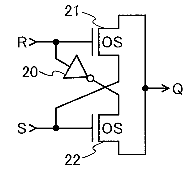
[0125]FIG. 9A is a circuit diagram illustrating a specific example of an SR latch circuit. The SR latch circuit in FIG. 9A includes an inverter 20, a transistor 21, and a transistor 22. An input terminal of the inverter 20 is electrically connected to a reset terminal (a first input terminal of the SR latch circuit in FIG. 9A, hereinafter also referred to as a terminal R). A gate of the transistor 21 is electrically connected to the terminal R. One of a source and a drain of the transistor 21 is electrically connected to a set terminal (a second input te...

first specific example

of Gated SR Latch Circuit

[0154]FIG. 20A is a circuit diagram illustrating a specific example of a gated SR latch circuit. The gated SR latch circuit in FIG. 20A includes a NAND gate 80, a NAND gate 81, an inverter 82, an inverter 83, a transistor 84, and a transistor 85. A first input terminal of the NAND gate 80 is electrically connected to a terminal E (a first input terminal of the gated SR latch circuit in FIG. 20A). A second input terminal of the NAND gate 80 is electrically connected to a terminal R (a second input terminal of the gated SR latch circuit in FIG. 20A). A first input terminal of the NAND gate 81 is electrically connected to the terminal E. A second input terminal of the NAND gate 81 is electrically connected to a terminal S (a third input terminal of the gated SR latch circuit in FIG. 20A). An input terminal of the inverter 82 is electrically connected to an output terminal of the NAND gate 80. An input terminal of the inverter 83 is electrically connected to an ...

second specific example

of Gated SR Latch Circuit

[0160]FIG. 22A is a circuit diagram illustrating a specific example of a gated SR latch circuit. The gated SR latch circuit in FIG. 22A includes a NAND gate 90, a NAND gate 91, a NAND gate 92, and a transistor 93. A first input terminal of the NAND gate 90 is electrically connected to a terminal E (a first input terminal of the gated SR latch circuit in FIG. 22A). A second input terminal of the NAND gate 90 is electrically connected to a terminal S (a second input terminal of the gated SR latch circuit in FIG. 22A). A first input terminal of the NAND gate 91 is electrically connected to the terminal E. A second input terminal of the NAND gate 91 is electrically connected to a terminal R (a third input terminal of the gated SR latch circuit in FIG. 22A). A first input terminal of the NAND gate 92 is electrically connected to an output terminal of the NAND gate 90. A second input terminal of the NAND gate 92 is electrically connected to an output terminal of t...


PUM


Abstract

The latch circuit includes a transistor whose channel region is formed with an oxide semiconductor (OS). Data is held in a node that is electrically connected to an output terminal and one of a source and a drain of the transistor and brought into a floating state when the transistor is turned off. Note that the oxide semiconductor has a band gap wider than silicon and an intrinsic carrier density lower than silicon. By using such an oxide semiconductor for the channel region of the transistor, the transistor with an extremely low off-state current (leakage current) can be realized.

Description

BACKGROUND OF THE INVENTION[0001]1. Field of the Invention[0002]The present invention relates to a latch circuit and a semiconductor device including the latch circuit. Note that the semiconductor device in this specification indicates any device that can operate by utilizing semiconductor characteristics.[0003]2. Description of the Related Art[0004]A latch circuit is a circuit that can temporarily hold a specific logic state (hereinafter also referred to as data), and is used in a variety of semiconductor devices. For example, a latch circuit is used as a circuit that temporarily hold data when the data is written or read to / from a storage circuit provided in a semiconductor device.[0005]The latch circuit can be constituted by logic gates. For example, there are an SR latch circuit illustrated in FIG. 26A, an / SR latch circuit illustrated in FIG. 26C, a JK latch circuit illustrated in FIG. 26E, a gated SR latch circuit illustrated in FIG. 26G, and a D latch circuit illustrated in F...

Claims


Application Information

Patent Timeline
Patent Type & Authority Applications(United States)
IPC IPC(8): H03K19/20
CPCH01L27/1156H01L27/11803H03K19/20H03K3/356H01L27/1225H10B41/70H01L27/1203
Inventor HATANO, TAKEHISA
Owner SEMICON ENERGY LAB CO LTD
Why Eureka
Try Eureka