Semiconductor compound structure and method of fabricating the same using graphene or carbon nanotubes, and semiconductor device including the semiconductor compound structure

a technology of graphene or carbon nanotubes and semiconductor compounds, which is applied in the direction of semiconductor/solid-state device manufacturing, semiconductor devices, electrical apparatus, etc., can solve the problems of difficult epitaxial growth of a group iii-v semiconductor compound and increase of fabrication costs

Active Publication Date: 2012-03-08
SAMSUNG ELECTRONICS CO LTD
View PDF10 Cites 41 Cited by
  • Summary
  • Abstract
  • Description
  • Claims
  • Application Information

AI Technical Summary

Benefits of technology

[0009]The substrate may include an amorphous substrate. The semiconductor compound structure may further include a wetting layer for easily depositing the semiconductor compound layer on the buffer layer.

Problems solved by technology

When light emitting devices are fabricated using a sapphire substrate or a silicon substrate, fabrication costs increase.
However, it is difficult to epitaxially grow a group III-V semiconductor compound such as gallium nitride (GaN) on the amorphous substrate.

Method used


Image

  • Semiconductor compound structure and method of fabricating the same using graphene or carbon nanotubes, and semiconductor device including the semiconductor compound structure
  • Semiconductor compound structure and method of fabricating the same using graphene or carbon nanotubes, and semiconductor device including the semiconductor compound structure
  • Semiconductor compound structure and method of fabricating the same using graphene or carbon nanotubes, and semiconductor device including the semiconductor compound structure

Examples


Embodiment Construction

[0029]Reference will now be made in detail to exemplary embodiments, examples of which are illustrated in the accompanying drawings, wherein like reference numerals refer to the like elements throughout. In this regard, the present exemplary embodiments may have different forms and should not be construed as being limited to the descriptions set forth herein. Accordingly, the exemplary embodiments are merely described below, by referring to the figures, to explain aspects of the present description.

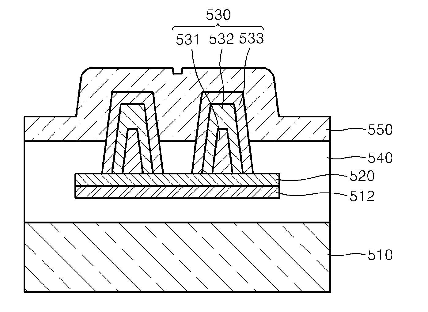
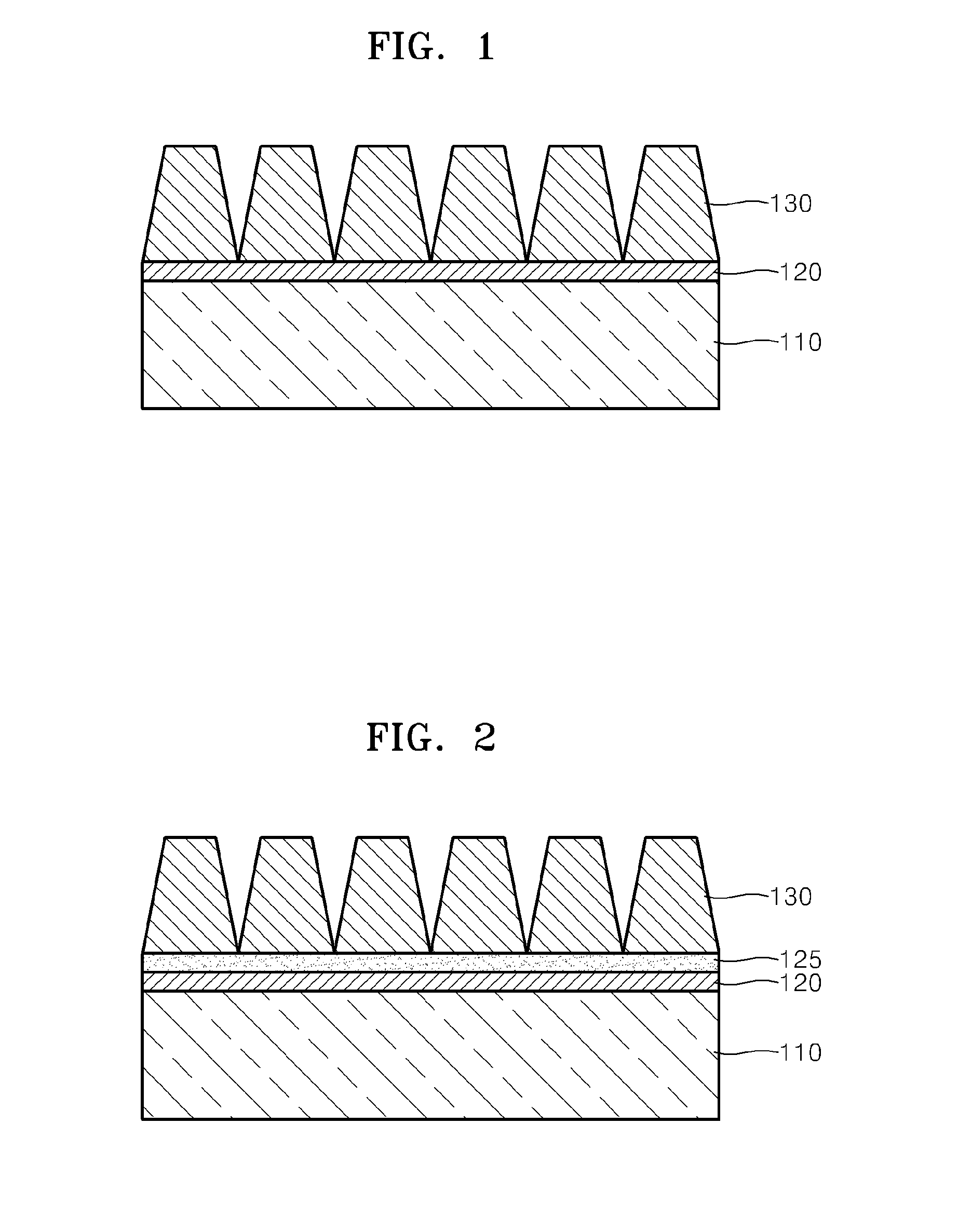
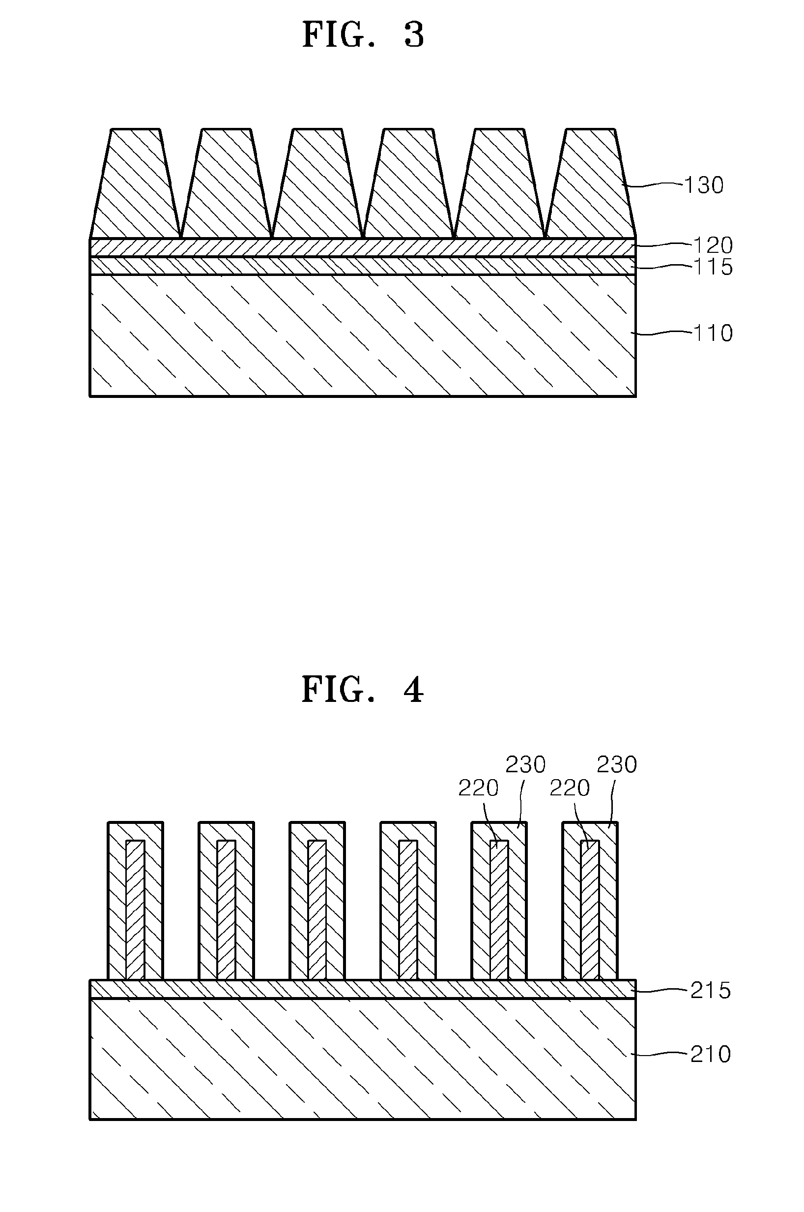
[0030]FIG. 1 is a cross-sectional view of a semiconductor compound structure according to an exemplary embodiment.

[0031]Referring to FIG. 1, the semiconductor compound structure of the present exemplary embodiment includes a substrate 110, a buffer layer 120 deposited on the substrate 110, and a semiconductor compound layer 130 formed on the buffer layer 120. In the present exemplary embodiment, the substrate 110 may be an amorphous substrate. For example, a glass substrate may be used as...


PUM

PropertyMeasurementUnit
temperatureaaaaaaaaaa
semiconductoraaaaaaaaaa

Abstract

A semiconductor compound structure and a method of fabricating the semiconductor compound structure using graphene or carbon nanotubes, and a semiconductor device including the semiconductor compound structure. The semiconductor compound structure includes a substrate; a buffer layer disposed on the substrate, and formed of a material including carbons having hexagonal crystal structures; and a semiconductor compound layer grown and formed on the buffer layer.

Description

CROSS-REFERENCE TO RELATED APPLICATIONS[0001]This application claims the benefit of Korean Patent Application No. 10-2010-0086586, filed on Sep. 3, 2010, in the Korean Intellectual Property Office, the disclosure of which is incorporated herein in its entirety by reference.BACKGROUND[0002]1. Field[0003]Exemplary embodiments consistent with the present disclosure relate to semiconductor compound structures and methods of manufacturing the same, and more particularly, to semiconductor compound structures and methods of manufacturing the semiconductor compound structures using graphene or carbon nanotubes, and semiconductor devices including the semiconductor compound structures.[0004]2. Description of the Related Art[0005]When light emitting devices are fabricated using a sapphire substrate or a silicon substrate, fabrication costs increase. To address the above problem, fabrication of light emitting devices by using an amorphous substrate such as a glass substrate has been tried. How...

Claims


Application Information

Patent Timeline
Patent Type & Authority Applications(United States)
IPC IPC(8): H01L33/30H01L29/20H01L21/20
CPCH01L21/02422H01L21/02444H01L33/24H01L29/1606H01L33/08H01L21/02538
Inventor CHOI, JUN-HEEKIM, UN-JEONGLEE, SANG-JIN
Owner SAMSUNG ELECTRONICS CO LTD
Why Eureka
Try Eureka