Package structure having MEMS element and fabrication method thereof

a technology of micro electro mechanical system and packaging structure, which is applied in the direction of microelectromechanical system, semiconductor device details, semiconductor/solid-state device details, etc., can solve the problems of low sensitivity, slow signal transmission, and excessive thickness of packaging structure, so as to reduce the thickness and volume of the overall structure, improve signal transmission efficiency, and reduce fabrication cost

Active Publication Date: 2012-03-08
SILICONWARE PRECISION IND CO LTD
View PDF3 Cites 12 Cited by
  • Summary
  • Abstract
  • Description
  • Claims
  • Application Information

AI Technical Summary

Benefits of technology

[0011]According to the present invention, the chip is directly embedded in the packaging substrate so as to reduce the thickness and volume of the overall structure. Further, since the chip, the MEMS element and the packaging substrate are electrically connected through embedded traces, the present invention improves the signal transmission efficiency and reduces the fabrication cost as compared to the wire bonding method of the prior art. In addition, the lid can be formed while forming the first conductive pads and the second conductive vias so as to simplify the fabrication process. Furthermore, as compared with the conventional QFN type lead frame, array-arranged solder balls of the present invention provide more I / O connections, thus expanding the application range of the present invention.

Problems solved by technology

However, due to the use of the lead frame 10 and the lid 13, the package structure becomes too thick.
Further, using the bonding wires made of gold for electrically connecting the MEMS element and the lead frame easily results in slow signal transmission and low sensitivity.
Also, gold wires incur high fabrication costs.
Furthermore, the encapsulant encapsulating the MEMS element and the gold wires leads to increase of the thickness of the overall package structure.
Therefore, such a package structure does not meet the trend of miniaturization and low cost.

Method used


Image

  • Package structure having MEMS element and fabrication method thereof
  • Package structure having MEMS element and fabrication method thereof
  • Package structure having MEMS element and fabrication method thereof

Examples


Embodiment Construction

[0014]The following illustrative embodiments are provided to illustrate the disclosure of the present invention, these and other advantages and effects can be apparent to those in the art after reading this specification.

[0015]It should be noted that the drawings are only for illustrative purposes and not intended to limit the present invention. Meanwhile, terms such as ‘up’, ‘down’, ‘a’ etc. are only used as a matter of descriptive convenience and not intended to have any other significance or provide limitations for the present invention.

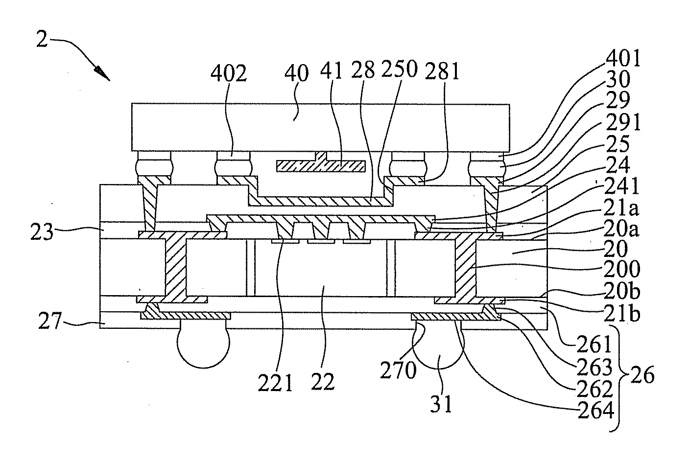
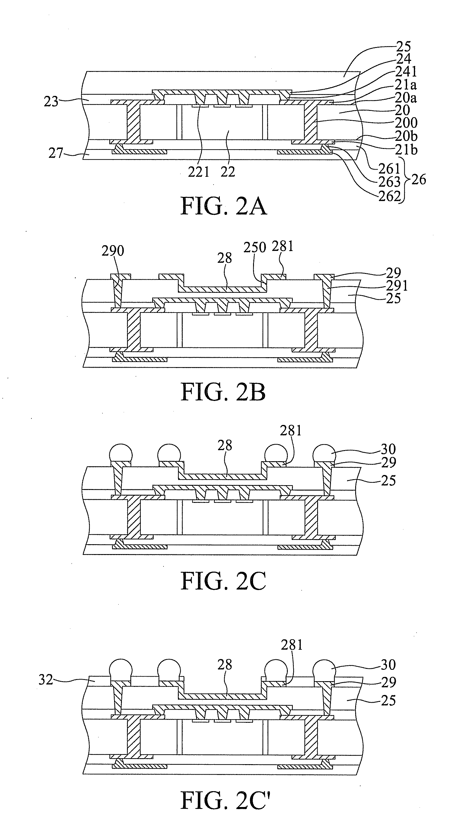
[0016]FIGS. 2A to 2E are cross-sectional views showing a package structure having an MEMS element and a fabrication method thereof according to the present invention.

[0017]Referring to FIG. 2A, a packaging substrate 20 having a first surface 20a and an opposite second surface 20b is prepared, wherein a first wiring layer 21a and a second wiring layer 21b are formed on the first surface 20a and the second surface 20b, respectively, and electrically...


PUM


Abstract

A package structure having an MEMS element includes: a packaging substrate having first and second wiring layers on two surfaces thereof and a chip embedded therein; a first dielectric layer disposed on the packaging substrate and the chip; a third wiring layer disposed on the first dielectric layer; a second dielectric layer disposed on the first dielectric layer and the third wiring layer and having a recessed portion; a lid disposed in the recessed portion and on the top surface of the second dielectric layer around the periphery of the recessed portion, wherein the portion of the lid on the top surface of the second dielectric layer is formed into a lid frame on which an adhering material is disposed to allow a substrate having an MEMS element to be attached to the packaging substrate with the MEMS element corresponding in position to the recessed portion, thereby providing a package structure of reduced size and costs with better electrical properties.

Description

BACKGROUND OF THE INVENTION[0001]1. Field of the Invention[0002]The present invention relates to package structures and fabrication methods thereof, and more particularly, to a package structure having a Micro Electro Mechanical System (MEMS) element and a fabrication method thereof.[0003]2. Description of Related Art[0004]Micro Electro Mechanical System (MEMS) techniques integrate electrical and mechanical functions into a single element using micro-fabrication technology. An MEMS element is disposed on a chip and covered by a shield or packaged with an underfill adhesive so as to protect the MEMS element from the external environment.[0005]FIG. 1 is a cross-sectional view of a conventional package structure having an MEMS element. Referring to FIG. 1, the package structure comprises a quad flat no lead (QFN) type lead frame 10; a chip 11 disposed on the lead frame 10; an MEMS element 12 disposed on the chip 11; a lid 13 disposed on the chip 11 to cover the chip 11; an aluminum lay...

Claims


Application Information

Patent Timeline
Patent Type & Authority Applications(United States)
IPC IPC(8): H01L29/84H01L21/50
CPCB81B7/007B81B2201/025B81B2207/096H01L23/5389H01L2924/09701H01L24/24H01L2224/45144H01L2224/32245H01L2224/48247H01L2224/73265H01L2224/16225H01L2924/1461H01L2924/3025H01L2924/00H01L2224/04105H01L2224/12105H01L2224/73267H01L2924/181H01L2924/14H01L2924/00012
Inventor HUANG, CHUN-ANLIAO, HSIN-YICHIU, SHIH-KUANG
Owner SILICONWARE PRECISION IND CO LTD
Why Eureka
Try Eureka