Semiconductor device

a technology of semiconductor devices and through electrodes, applied in semiconductor devices, semiconductor/solid-state device details, electrical equipment, etc., can solve the problems of thermal stress, deterioration of semiconductor devices such as semiconductor chips, and increased signal delays, so as to reduce the cost of forming through electrodes and reduce thermal stress. , the effect of a relatively high temperature of the beol process

Active Publication Date: 2012-03-08
SAMSUNG ELECTRONICS CO LTD
View PDF3 Cites 70 Cited by
  • Summary
  • Abstract
  • Description
  • Claims
  • Application Information

AI Technical Summary

Benefits of technology

[0033]Accordingly, a thermal stress to a through electrode under a relatively high temperature of the BEOL process may be reduced. In addition, the resultant through electrode may be formed to have a desired length. Further, costs for forming the through electrode may be reduced, and during the manufacturing processes, a conductive material such as copper may be prevented from diffusing into the substrate.

Problems solved by technology

As device speeds and device integration increase, signal delays may also be increased, for example, due to parasitic capacitance introduced by interconnection structures.
Especially, when the portion of the conductive metal layer is exposed during an etch process, the metal of the conductive metal layer such as copper may diffuse into the substrate, thereby deteriorating a semiconductor device such as a semiconductor chip.
Further, a thermal stress may occur due to a thermal expansion difference between the metal and the substrate.
Thus, it may be relatively difficult to form the opening having a desired aspect ratio in the substrate.

Method used


Image

  • Semiconductor device
  • Semiconductor device
  • Semiconductor device

Examples


Embodiment Construction

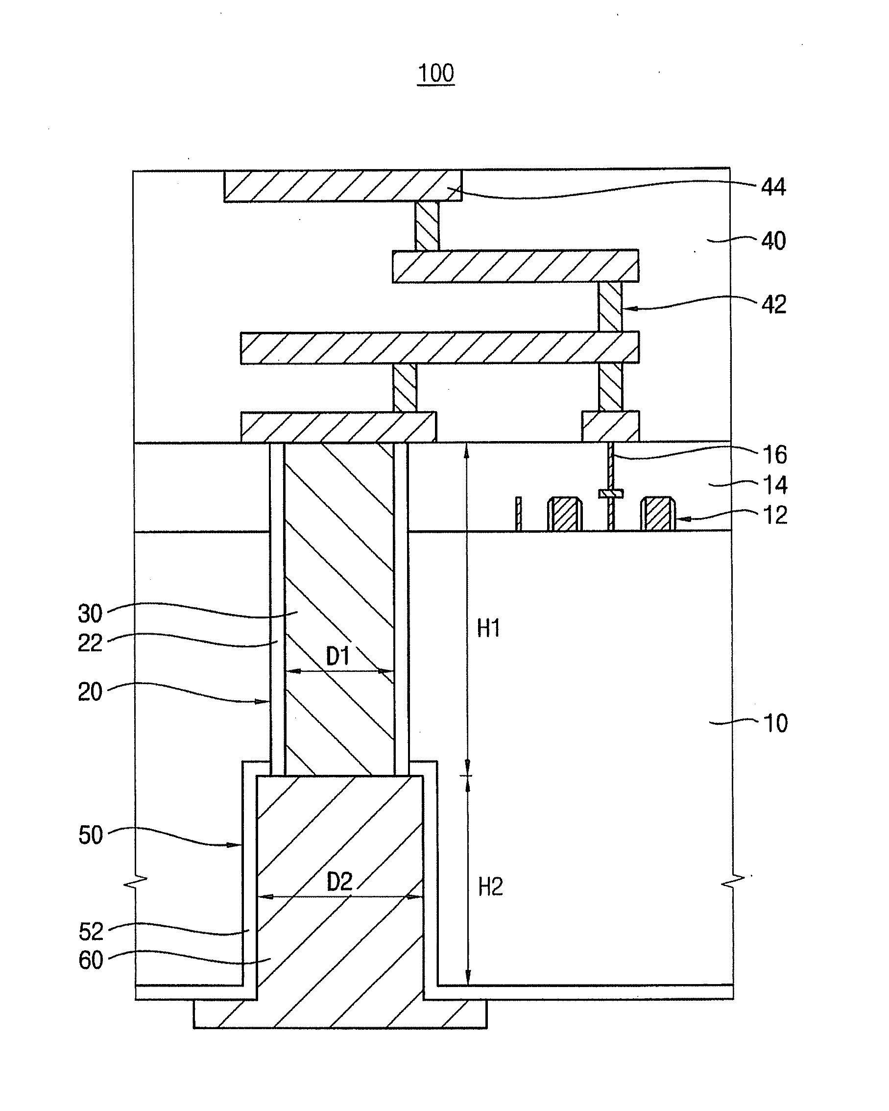
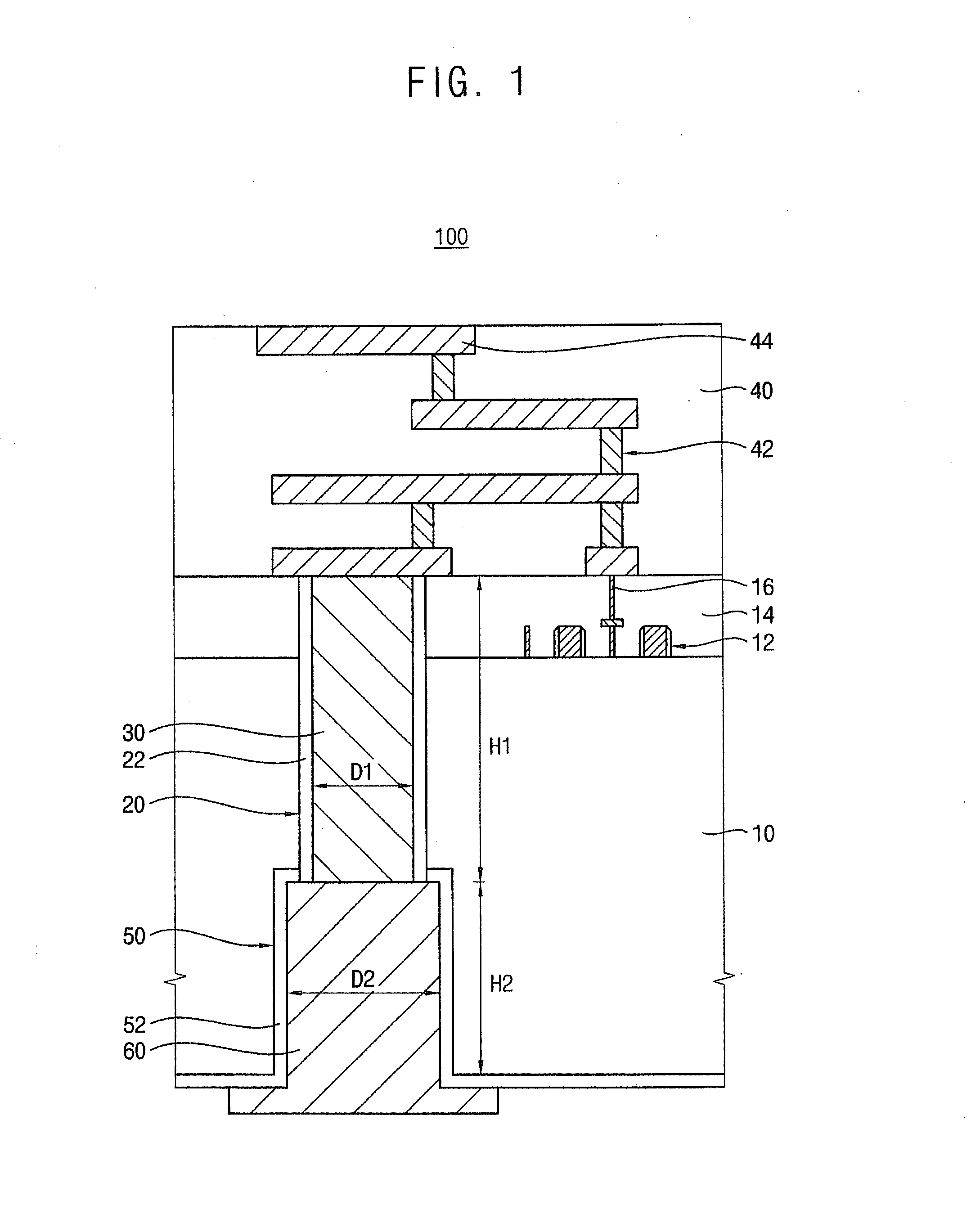
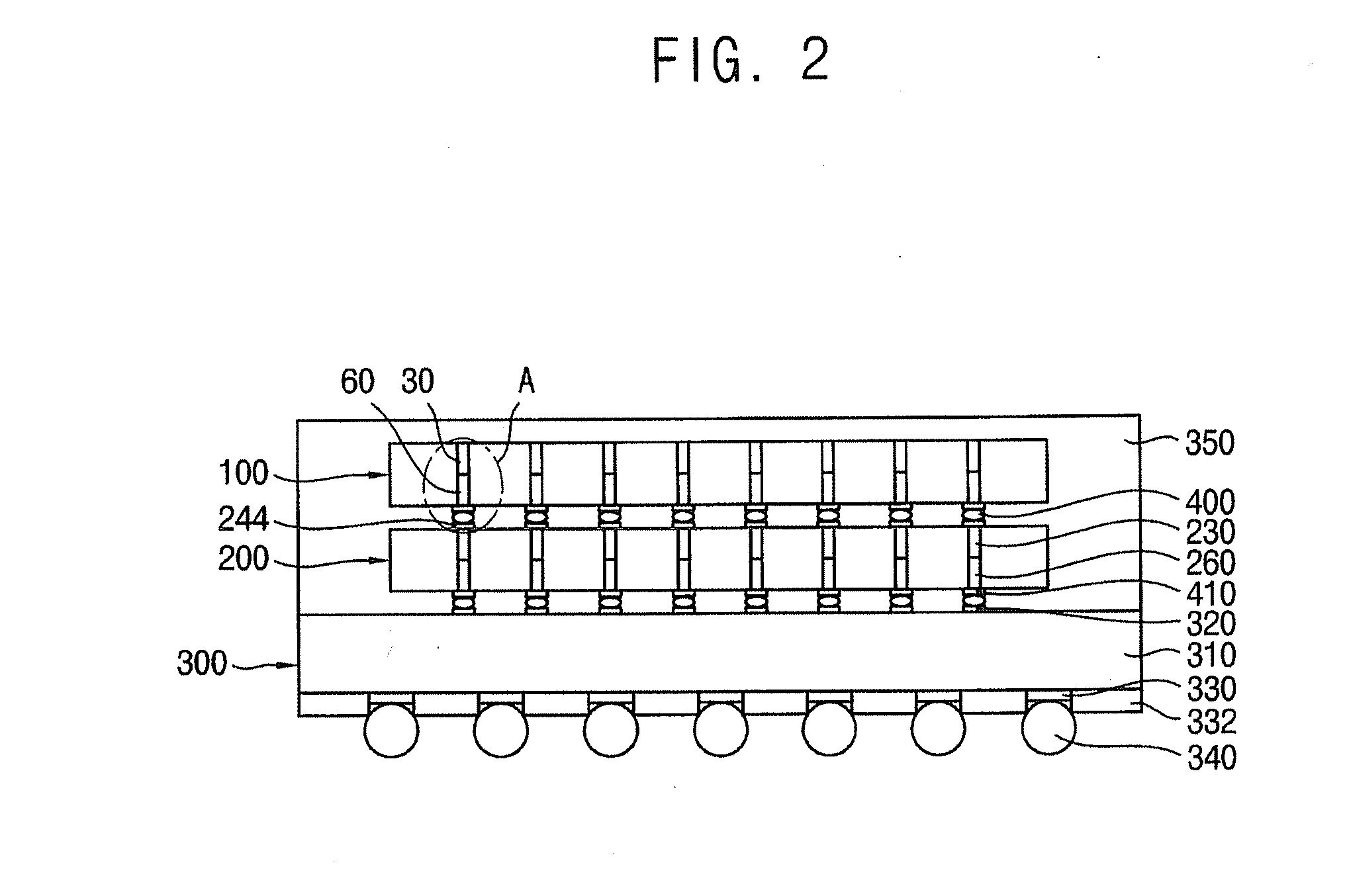
[0043]Various example embodiments will be described more fully hereinafter with reference to the accompanying drawings, in which example embodiments are shown. Example embodiments may, however, be embodied in many different forms and should not be construed as limited to example embodiments set forth herein. Rather, these example embodiments are provided so that this disclosure will be thorough and complete, and will fully convey the scope of example embodiments to those skilled in the art. In the drawings, the sizes and relative sizes of layers and regions may be exaggerated for clarity.

[0044]It will be understood that when an element or layer is referred to as being “on,”“connected to” or “coupled to” another element or layer, it can be directly on, connected or coupled to the other element or layer or intervening elements or layers may be present. In contrast, when an element is referred to as being “directly on,”“directly connected to” or “directly coupled to” another element or...


PUM


Abstract

A semiconductor device may include a substrate and a through electrode. The substrate may have a first surface and a second surface opposite to the first surface, the substrate including circuit patterns formed on the first surface. The through electrode penetrates the substrate and may be electrically connected to the circuit pattern, the through electrode including a first plug that extends from the first surface in a thickness direction of the substrate and a second plug that extends from the second surface in the thickness direction of the substrate so as to be connected to the first plug.

Description

PRIORITY STATEMENT[0001]This application claims priority under 35 U.S.C. §119 to Korean Patent Application No. 10-2010-0087233, filed on Sep. 7, 2010 in the Korean Intellectual Property Office (KIPO), the entire contents of which are herein incorporated by reference.BACKGROUND[0002]1. Field[0003]Example embodiments relate to a semiconductor device and a method of manufacturing a semiconductor device. More particularly, example embodiments relate to a semiconductor device having a through electrode in a semiconductor substrate and / or a method of manufacturing the semiconductor device.[0004]2. Description of the Related Art[0005]As device speeds and device integration increase, signal delays may also be increased, for example, due to parasitic capacitance introduced by interconnection structures. Advances in integration technology have led to the development of three-dimensional integration, where wafers may be stacked three-dimensionally, in contrast to the conventional two-dimension...

Claims


Application Information

Patent Timeline
Patent Type & Authority Applications(United States)
IPC IPC(8): H01L23/48
CPCH01L21/76898H01L23/481H01L2924/15311H01L2224/16225H01L2224/16145
Inventor LEE, HO-JINCHO, SUNG-DONGJEONG, SE-YOUNGPARK, YEONG-LYEOLKANG, SIN-WOO
Owner SAMSUNG ELECTRONICS CO LTD
Why Eureka
Try Eureka