Method and system for hybrid integration of a tunable laser and a phase modulator

a phase modulator and tunable laser technology, applied in semiconductor lasers, laser details, electrical equipment, etc., can solve the problems of limited integration of advanced electrical functions on silicon, inconvenient laser linewidth, and inability to manufacture monolithically integrated opto-electronic integrated circuits, etc., to reduce the size and power consumption of optical communication systems, improve the laser linewidth, and minimize the effect of refractive index fluctuations

Inactive Publication Date: 2012-03-08
SKORPIOS TECH
View PDF3 Cites 65 Cited by
  • Summary
  • Abstract
  • Description
  • Claims
  • Application Information

AI Technical Summary

Benefits of technology

[0010]Numerous benefits are achieved by way of the present invention over conventional techniques. For example, embodiments of the present invention provide methods and systems suitable for reducing the size and power consumption of optical communications systems, relaxing the requirements for stringent tem

Problems solved by technology

Silicon has not been useful for light emission or optical amplification due to its indirect energy bandgap.
This deficiency has prevented the fabrication of monolithically integrated opto-electronic integrated circuits on sili

Method used


Image

  • Method and system for hybrid integration of a tunable laser and a phase modulator
  • Method and system for hybrid integration of a tunable laser and a phase modulator
  • Method and system for hybrid integration of a tunable laser and a phase modulator

Examples


Embodiment Construction

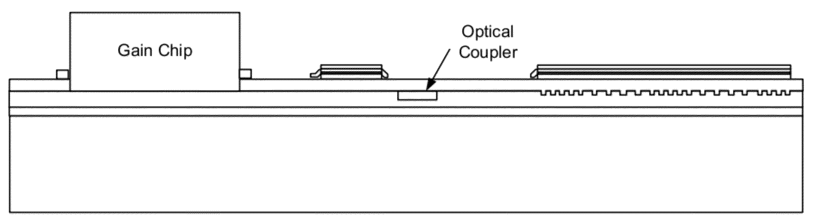
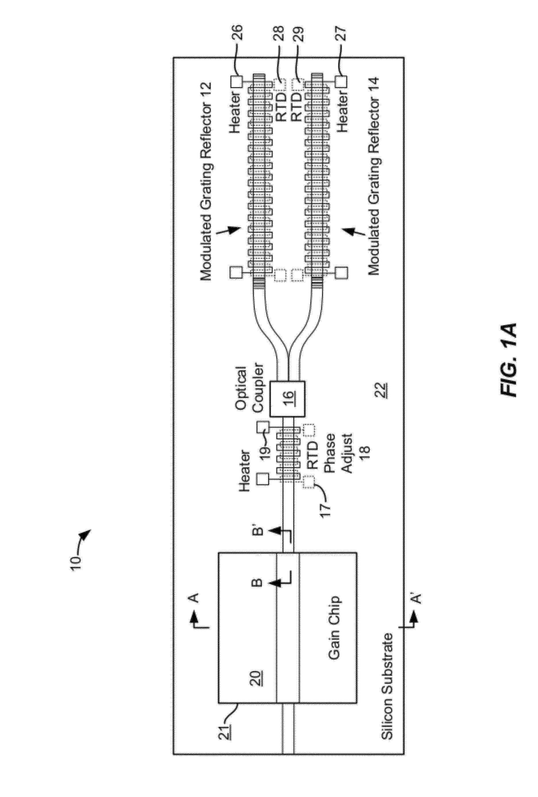
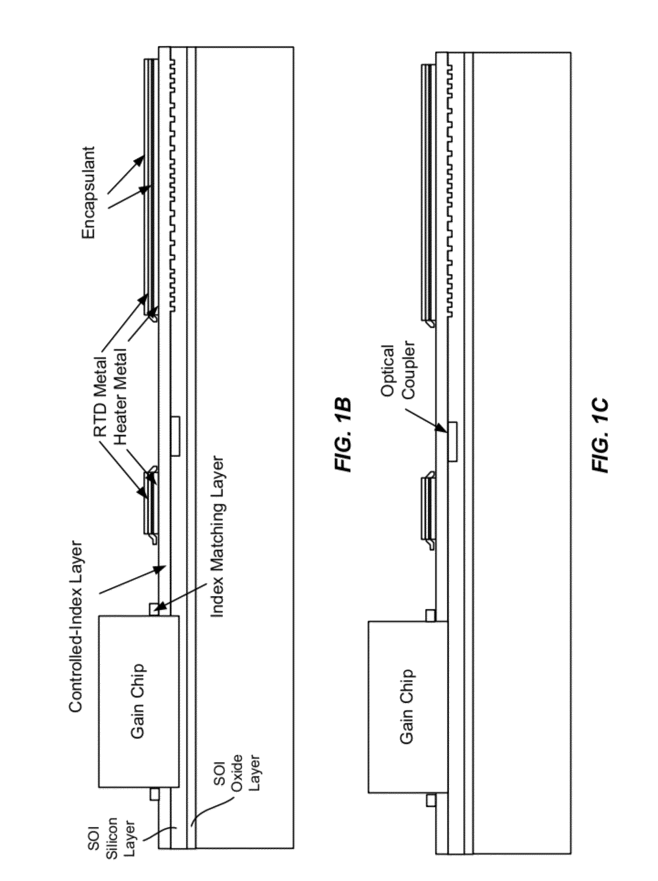
[0032]Hybrid integration on silicon is preferable for the commercial deployment of optoelectronic integrated circuits. Silicon is a preferable material for electronic integration. Silicon technology has advanced such that extremely complex electronic functions can be realized very inexpensively. Silicon is also a good material for constructing low loss optical waveguides. However, monolithic integration of light generating or detecting functions has been prevented in silicon because it is an indirect bandgap material. Conversely, compound semiconductor materials, including III-V materials such as indium phosphide are well suited for light generation and detection because of their physical properties such as being direct bandgap materials. These materials are complex material systems with small substrates and relatively (compared to silicon) low yields. As such, constructing devices with a high level of functionality is currently cost prohibitive.

[0033]Embodiments of the present inve...


PUM


Abstract

A tunable laser includes a substrate comprising a silicon material and a gain medium coupled to the substrate. The gain medium includes a compound semiconductor material. The tunable laser also includes an optical modulator optically coupled to the gain medium, a phase modulator optically coupled to the optical modulator, and a waveguide disposed in the substrate and optically coupled to the gain medium. The tunable laser further includes a first wavelength selective element characterized by a first reflectance spectrum and disposed in the substrate, a second wavelength selective element characterized by a second reflectance spectrum and disposed in the substrate, an optical coupler disposed in the substrate and joining the first wavelength selective element, the second wavelength selective element, and the waveguide, and an output mirror.

Description

CROSS-REFERENCES TO RELATED APPLICATIONS[0001]This present application is a continuation-in-part of U.S. patent application Ser. No. 12 / 903,025, filed on Oct. 12, 2010, which claims priority to U.S. Provisional Patent Application No. 61 / 251,143, filed on Oct. 13, 2009, the disclosures of which are hereby incorporated by reference in their entirety for all purposes. U.S. patent application Ser. No. 12 / 903,025 was filed concurrently with 12 / 902,621, the disclosure of which is hereby incorporated by reference in its entirety for all purposes.BACKGROUND OF THE INVENTION[0002]Advanced electronic functions such as photonic device bias control, modulation, amplification, data serialization and de-serialization, framing, routing, and other functions are typically deployed on silicon integrated circuits. A key reason for this is the presence of a global infrastructure for the design and fabrication of silicon integrate circuits that enables the production of devices having very advanced func...

Claims


Application Information

Patent Timeline
IPC IPC(8): H01S3/10
CPCH01S3/10053H01S3/1055H01S3/107H01S5/021H01S2301/03H01S5/02272H01S5/1003H01S5/1032H01S5/141H01S5/02248H01S5/02325H01S5/0237
Inventor DALLESASSE, JOHNKRASULICK, STEPHEN B.KOZLOVSKY, WILLIAM
Owner SKORPIOS TECH
Why Eureka
Try Eureka