Scanning probe having integrated silicon tip with cantilever

a technology of cantilever and scanning probe, which is applied in the direction of instruments, transportation and packaging, paper/cardboard containers, etc., can solve the problems of high level of control, difficult to define the exact thickness of the membrane, and inherent process difficulties

Active Publication Date: 2012-03-08
APPLIED NANOSTRUCTURES INC
View PDF5 Cites 24 Cited by
  • Summary
  • Abstract
  • Description
  • Claims
  • Application Information

AI Technical Summary

Benefits of technology

[0008]The current invention address the drawbacks mentioned above in the prior-art technology. The various aspects of the invention provide a robust and economical process for batch fabricating a plurality of cantilever assemblies, each having a sharp, self-aligned tetrahedral tip at the extreme end of cantilever. The invention allows the requirement of only two mask step for fabricating a complete scanning probe assembly including cantilever, tip, and holding chip, compared with three or more mask steps in the prior art. The process may rely upon standard processes for micro-electro-mechanic systems (MEMS).

Problems solved by technology

Although the Akamine process is very robust, it presents some inherent process difficulties.
The definition of the membrane of exact thickness becomes very difficult and requires high level of control during wet etching.
Lithography on a thin silicon membrane is very difficult, and the chances of wafer breakage are also very high during the lithography process.
The method also requires precise alignment for selectively removing nitride from the cantilever to form the tip by anisotropic etching, which again is a drawback in batch fabrication of the cantilever chip with precision.
Another limitation is the inherent inability of this process to fabricate rectangular single crystal silicon cantilevers, thus limiting its use to fabricate thin film cantilevers for a restricted set of applications.
Though Toda's method addresses the problem evident in Akamine et al. of controlling the thickness of the membrane by using an etch stop layer, it still requires a lithography to be performed on a thin silicon layer to etch the hole.
Hence, handling of the wafer becomes very critical during the lithography step.
Also the method does not address the inability of previous processes of fabricating rectangular cantilevers made of single crystal silicon.
Though Toda proposes an embodiment to fabricate silicon cantilevers using heavily doped boron layer as the etch stop layer and later using this layer for the cantilever, the implementation of such a scheme is expensive and complex, which increases the cost of mass fabrication.

Method used


Image

  • Scanning probe having integrated silicon tip with cantilever
  • Scanning probe having integrated silicon tip with cantilever
  • Scanning probe having integrated silicon tip with cantilever

Examples


Embodiment Construction

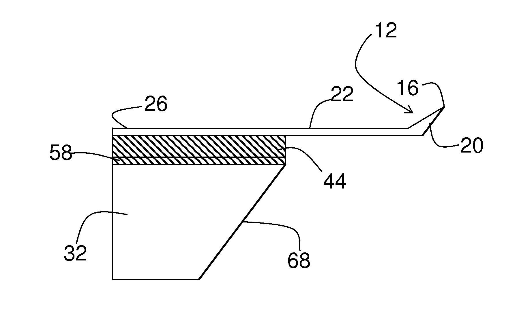
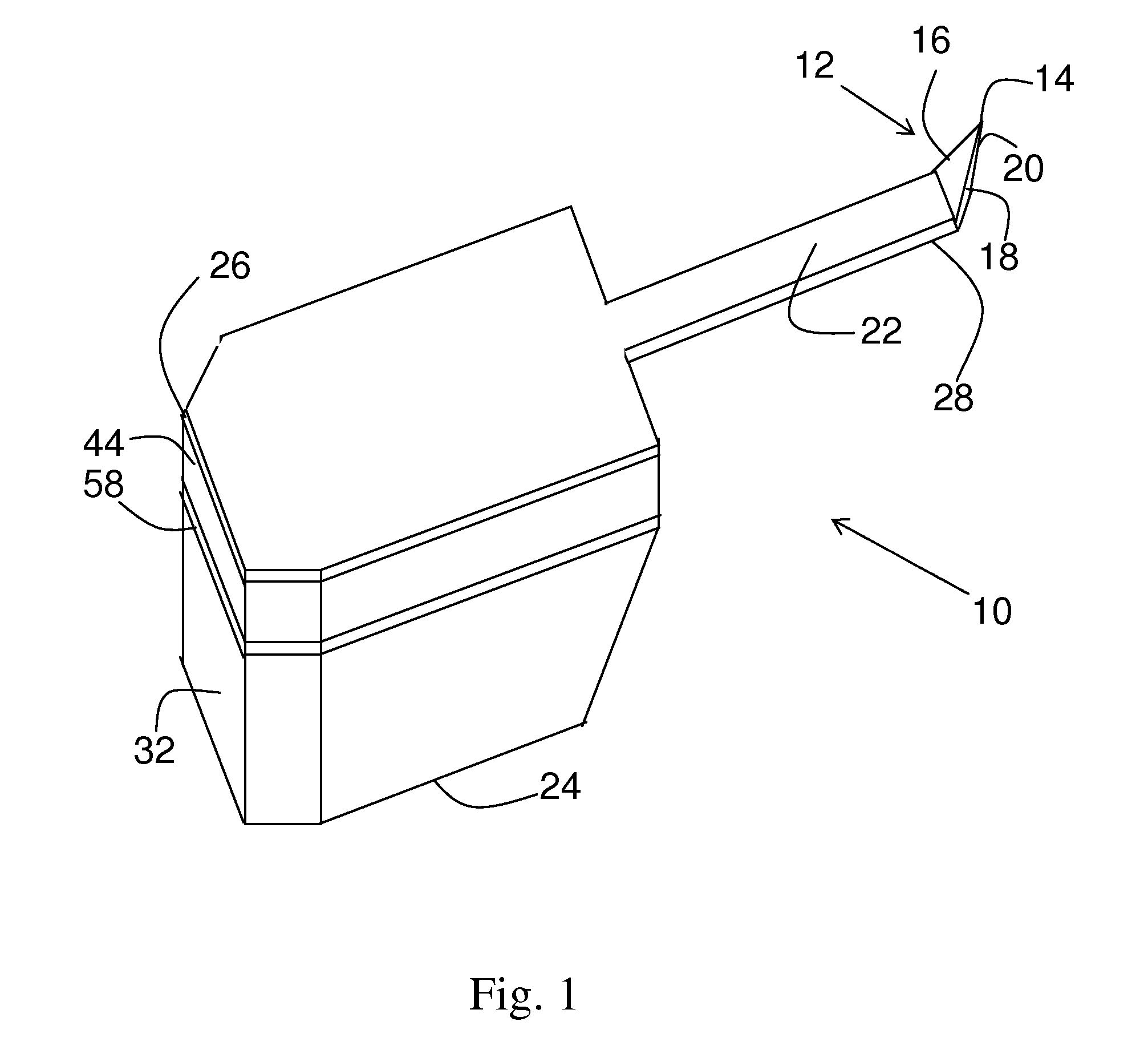
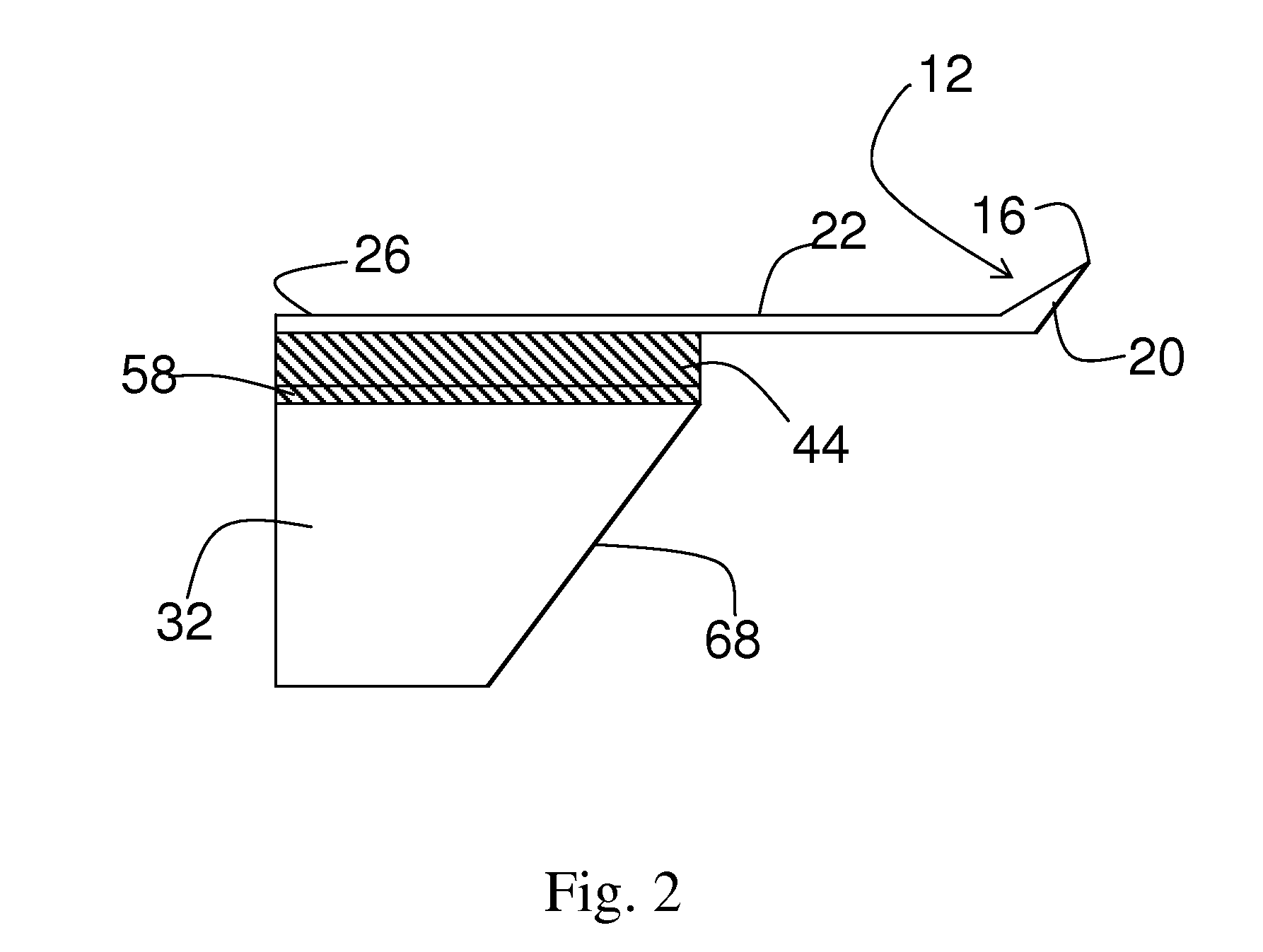
[0029]A probe assembly 10 of a first embodiment of the invention, illustrated in the orthographic view of FIG. 1 and the sectioned view of FIG. 2, may be formed by conventional processes well known for micro-electromechanical systems (MEMS). A triangular (tetrahedral) tip 12 terminating in a sharp apex 14 is formed of a first inclined surface 16 and two second inclined surfaces 18 separated by an inclined corner 20. The tip 12 extends upwardly and outwardly from a free or distal end of a cantilever 22, the fixed or proximal end of which is attached to and supported by a support 24. In this embodiment, the cantilever 22 is continuous with a cantilever layer 26 on top of the support 24. In use, the tip 12 points downwardly toward a sample being probed, but the opposite orientation is used here to clearly show the tip 12 and its formation. The support 24 is only partially illustrated and typically forms a support frame having an aperture over which the cantilever 22 and attached tip 12...


PUM

PropertyMeasurementUnit
angleaaaaaaaaaa
angleaaaaaaaaaa
angleaaaaaaaaaa

Abstract

A cantilever-tip assembly for atomic force microscopy (AFM) or other scanning probe microscopy and its method of making based on micro-electromechanical systems (MEMS). Two crystalline silicon wafers and attached oxide and nitride layers are bonded together across an intermediate dielectric layer. A thin cantilever with a tetrahedral silicon probe tip at its distal end are formed in one wafer by anisotropic etching of silicon and a support structure is formed in the other wafer to support the proximal end of the cantilever preferably having an inclined face formed by anisotropic silicon etching. The cantilever may be silicon or silicon nitride.

Description

FIELD OF THE INVENTION[0001]This invention relates generally to a fabrication method utilizing micro-electro-mechanical system (MEMS) processes to develop a sharp single crystal silicon tip at the free end of a micro cantilever, which can be made of single crystal silicon or other thin films, for use in scanning probe microscopes and other related microscopy systems.BACKGROUND ART[0002]Atomic force microscopy (AFM) allows high resolution surface imaging by scanning a sharp tip over a surface while controlling the interaction force between the tip and surface. AFM typically relies on a micromachined cantilever with a sharp tip at the distal or free end of the cantilever as a force sensor to detect the interaction between the tip and the sample. The force of the interaction of the tip is sensed by the resultant deflection of the cantilever on which the tip is mounted. The role of the cantilever is to translate the force acting on the tip into a deflection that can be subsequently moni...

Claims


Application Information

Patent Timeline
Patent Type & Authority Applications(United States)
IPC IPC(8): G01Q70/08B32B38/10B32B37/00
CPCB82Y35/00Y10T156/10G01Q70/10G01Q60/38
Inventor PODDAR, RAKESHCHAND, AMI
Owner APPLIED NANOSTRUCTURES INC
Why Eureka
Try Eureka