

Liquid crystal display device
a crystal display and liquid crystal technology, applied in semiconductor devices, instruments, optics, etc., can solve the problems of reducing the aperture ratio of the pixel, the need to increase the channel width of the pixel transistor, and the difficulty of ensuring the appropriate storage capacitor in the small-area pixel, so as to achieve higher-definition image display and reduce power consumption
- Summary
- Abstract
- Description
- Claims
- Application Information
AI Technical Summary
Benefits of technology
Problems solved by technology
Method used
Image

Examples
embodiment 1
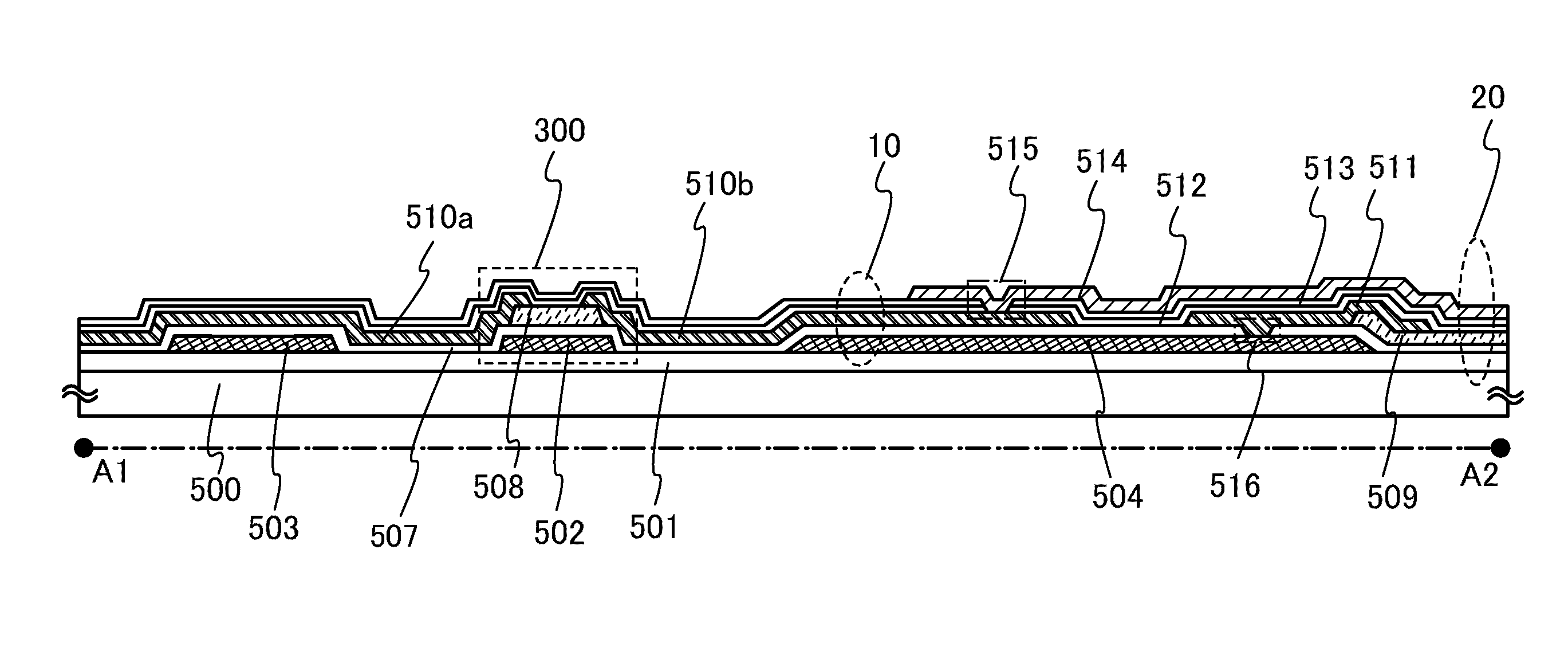
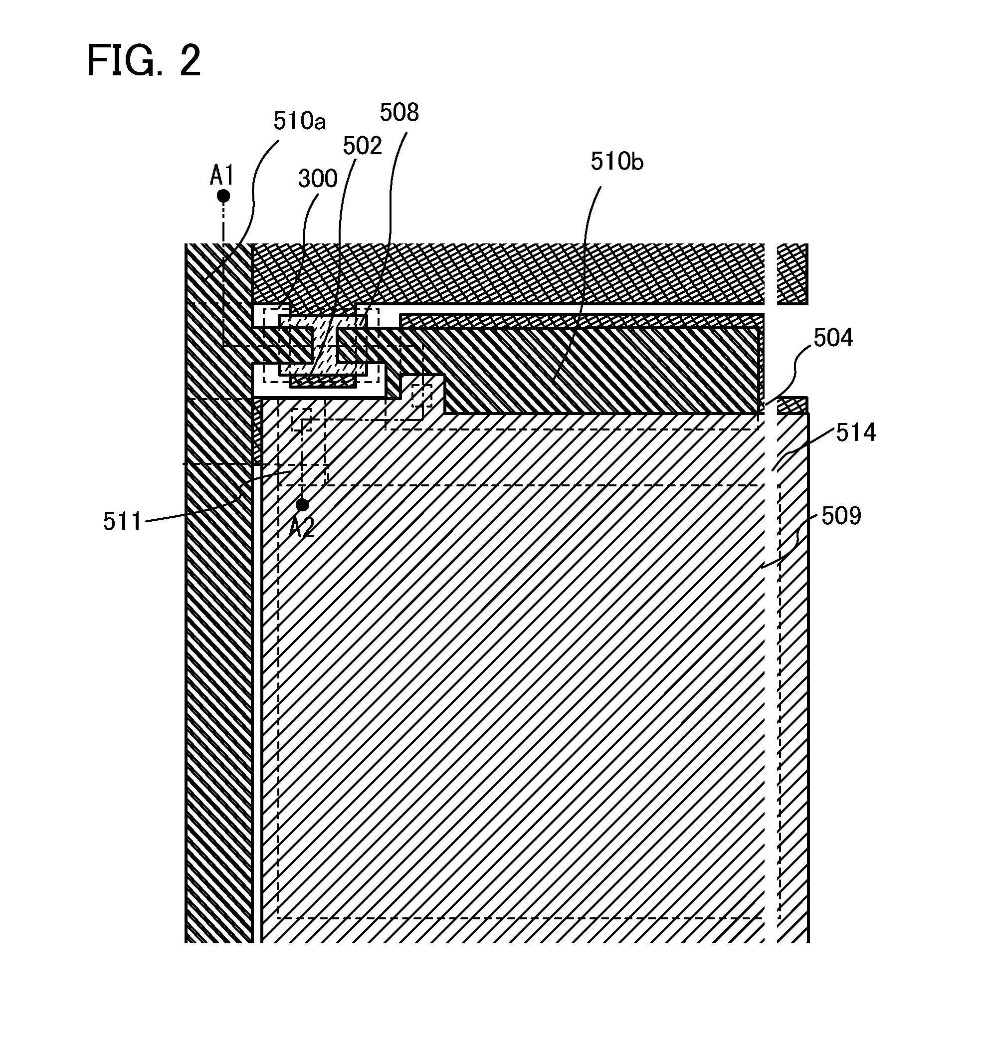
[0031]In the present embodiment, a pixel structure and a method for switching the storage capacitors will be described in a liquid crystal display device according to an embodiment of the present invention disclosed herein. It is to be noted that the liquid crystal display device described in the present embodiment includes pixels each with a variable capacitance value in response to images displayed.
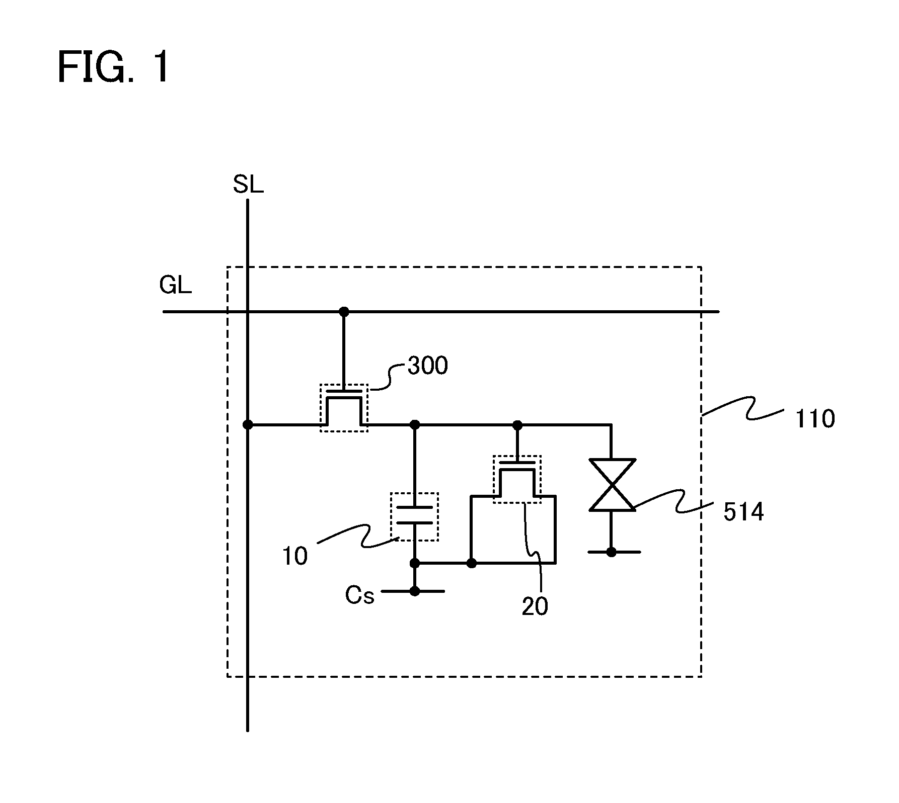
[0032]FIG. 1 is a diagram illustrating a circuit example of a pixel included in the liquid crystal display device.
[0033]A pixel 110 includes a pixel transistor 300, a first capacitive element 10, and a second capacitive element 20. The pixel transistor 300 has a gate electrode electrically connected to a scan line GL, and a first electrode electrically connected to a signal line SL, which serves as one of a source electrode and a drain electrode of the pixel transistor 300. Furthermore, one electrode of the first capacitive element 10 is electrically connected to one electrode of the se...
embodiment 2
[0060]In the present embodiment, another pixel structure and a method for switching the storage capacitors will be described in a liquid crystal display device according to an embodiment of the present invention disclosed herein. It is to be noted that the liquid crystal display device described in the present embodiment includes pixels each with a variable capacitance value in response to images displayed.
[0061]FIG. 6 is a diagram illustrating a circuit example of a pixel included in the liquid crystal display device.
[0062]A pixel 111 includes a pixel transistor 301, a transistor 400, a first capacitive element 11, and a second capacitive element 21. The pixel transistor 301 has a gate electrode electrically connected to a scan line GL, and a first electrode electrically connected to a signal line SL, which serves as one of a source electrode and a drain electrode of the pixel transistor 301. Furthermore, one electrode of the first capacitive element 11 is electrically connected to...
PUM
 Abstract
Description
Claims
Application Information