Monolithic microwave integrated circuit

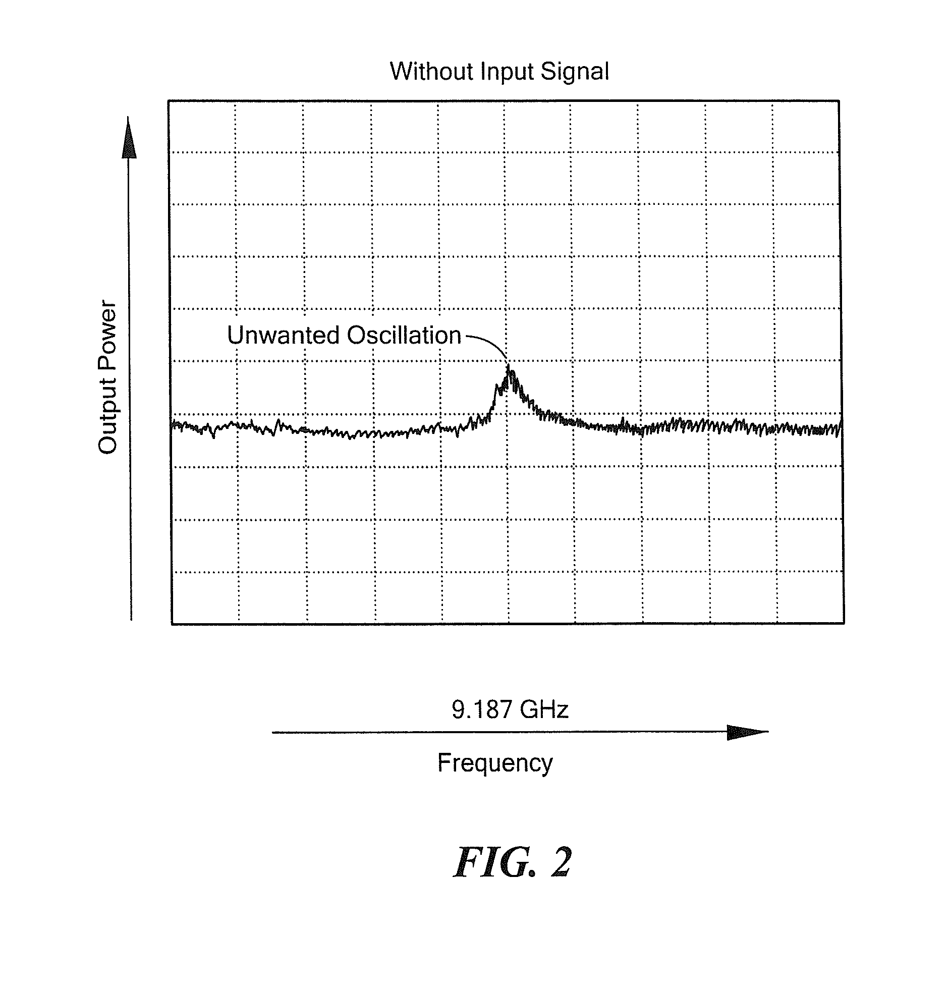
a technology of integrated circuits and monolithic microwaves, applied in the association of printed circuit non-printed electric components, waveguides, electrical apparatus contruction details, etc., can solve problems such as interference, interference, and unwanted amplifier oscillation

Active Publication Date: 2012-03-15
RAYTHEON CO
View PDF2 Cites 21 Cited by
  • Summary
  • Abstract
  • Description
  • Claims
  • Application Information

AI Technical Summary

Benefits of technology

[0002]As is known in the art, monolithic microwave integrated circuits (MMICs) have a wide range of applications. Typically a plurality of active devices (e.g., field effect transistors (FETs)) are formed in a semiconductor substrate structure and th

Problems solved by technology

We have found that this added metalized surface, in conjunction with the topside metal used for the ground plane of the CPW, forms a two-conductor, parallel plate, system that can support waveguide modes that generate feedback around the amplifiers interconnected by the CPW transmission line resulting in unwanted amplifier oscillation.
If the resonance frequency associated with this mode falls within the frequency of operation of the amplifier circuit then it may hinder the proper operation of the circuit.
This mode also may disrupt the proper circuit operation in the same way described above.

Method used


Image

  • Monolithic microwave integrated circuit
  • Monolithic microwave integrated circuit
  • Monolithic microwave integrated circuit

Examples


Embodiment Construction

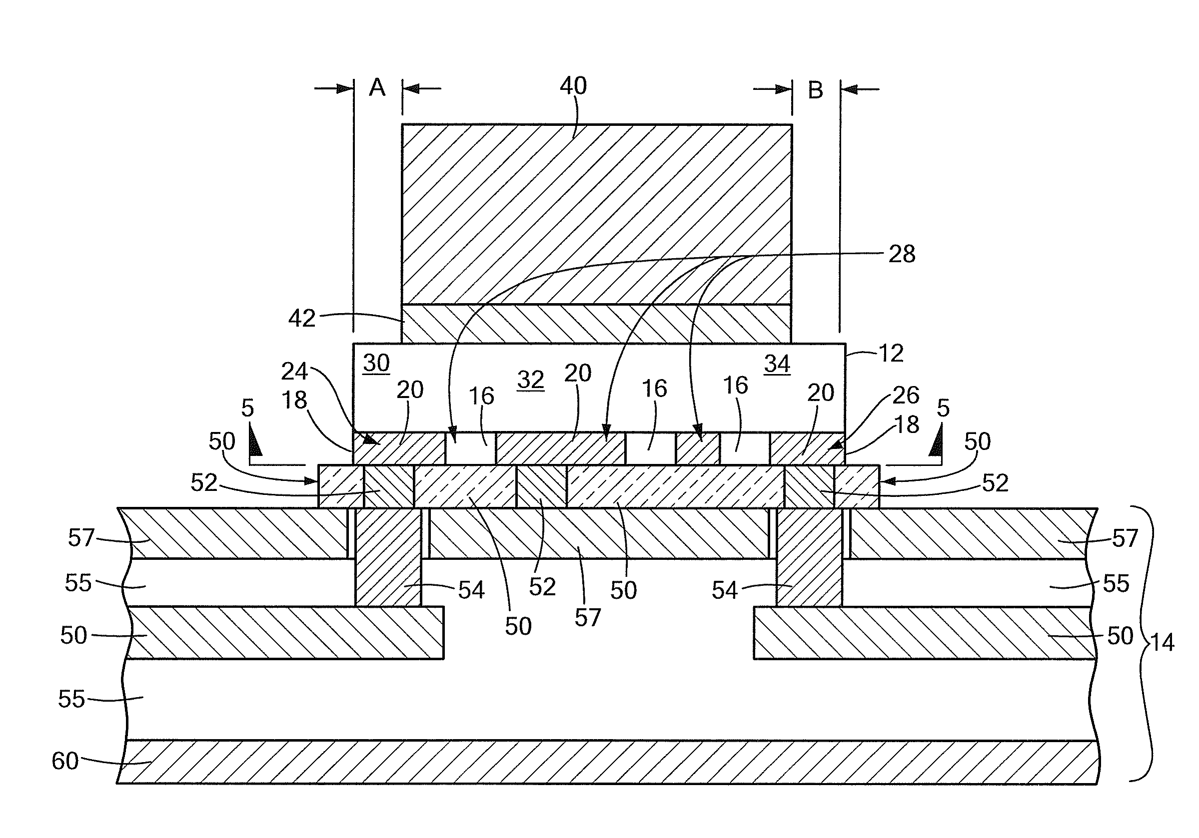
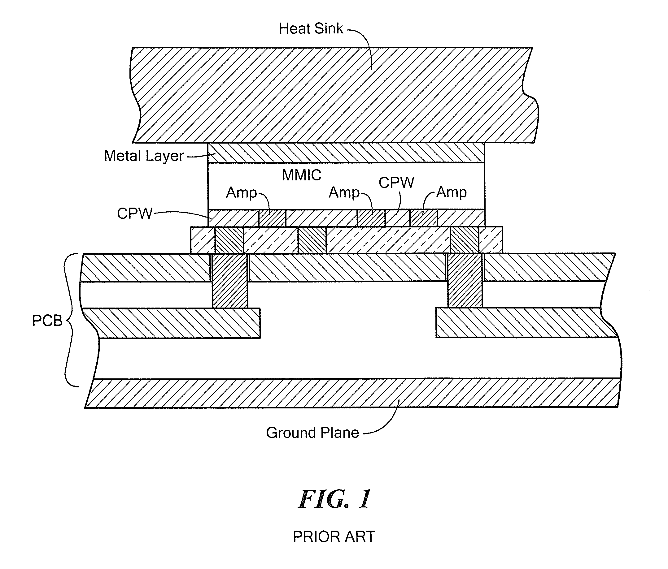
[0017]Referring now to FIGS. 3, 4 and 5, a monolithic microwave integrated circuit (MMIC) structure 10 is shown. The structure 10 includes an MMIC chip 12 mounted on the printed circuit board (PCB) 14 in flip-chip configuration. The MMIC structure 10 includes: a semiconductor substrate structure 12, here for example, GaN having a plurality of active devices (e.g., transistors) formed in a bottom surface portion of the substrate structure 12, here arranged as a plurality of, here, for example, three microwave amplifiers 16 (FIG. 5); and a microwave transmission line 18, here for example, a coplanar waveguide (CPW) microwave transmission line, formed on the bottom surface of the substrate structure 12. As is known, the CPW has strip conductors 20 separated from a coplanar ground plane conductor 22 by portions of the semiconductor substrate 12. The CPW has an input section 24, an output section 26 and a interconnecting section 26 electrically connected between the input section and the...


PUM


Abstract

A monolithic microwave integrated circuit structure having a semiconductor substrate structure with a plurality of active devices and a microwave transmission line having an input section, an output section and a interconnecting section electrically interconnecting the active devices on one surface and a metal layer on an opposite surface overlaying the interconnection section and absent from overlaying at least one of the input section and the output section.

Description

TECHNICAL FIELD[0001]This disclosure relates generally to monolithic microwave integrated circuits (MMICs) and more particularly to MMICs having heat sinks.BACKGROUND AND SUMMARY[0002]As is known in the art, monolithic microwave integrated circuits (MMICs) have a wide range of applications. Typically a plurality of active devices (e.g., field effect transistors (FETs)) are formed in a semiconductor substrate structure and the devices interconnected with microwave transmission lines, also formed on the substrate structure, to form, for example, a plurality of interconnected amplifiers. One type of microwave transmission line is coplanar waveguide (CPW) transmission line.[0003]As is also known in the art, for certain high power applications the bottom side of the CPW MMIC is metalized so that a heat sink can be attached as shown in FIG. 1. We have found that this added metalized surface, in conjunction with the topside metal used for the ground plane of the CPW, forms a two-conductor,...

Claims


Application Information

Patent Timeline
IPC IPC(8): H05K7/20H05K7/06
CPCH01L23/36H01L23/42H01L23/66H01L2223/6627H01L2924/19033H01L2224/131H01L2224/16225H01L2224/16235H01L2224/291H01L2224/32225H01L2224/73204H01L2224/73253H01L2924/1423H01L2223/6683H05K1/0203H05K2201/09985H05K2201/10166H05K1/0243H05K2201/10977H05K1/115H01P5/08H01L2924/00014H01L2924/014H01L2924/00H01L23/34
Inventor REZA, SHAHEDSWIDERSKI, EDWARDALM, ROBERTO W.
Owner RAYTHEON CO
Why Eureka
Try Eureka