Gallium nitride based semiconductor devices and methods of manufacturing the same

a technology of gallium nitride and semiconductor devices, which is applied in the direction of semiconductor devices, diodes, electrical apparatus, etc., can solve the problems of increasing the overall cost of manufacturing gan-based semiconductor devices, gan-based semiconductor devices do not have excellent heat dissipation characteristics, and the sic substrate is relatively expensive (about 10 times more expensive), so as to achieve good heat dissipation characteristics, improve current spreading characteristics, and reduce the cost of manufacturing

Inactive Publication Date: 2012-03-29
SAMSUNG ELECTRONICS CO LTD
View PDF9 Cites 8 Cited by
  • Summary
  • Abstract
  • Description
  • Claims
  • Application Information

AI Technical Summary

Benefits of technology

[0008]Example embodiments of the present invention provide gallium nitride base semiconductor devices which may have an excellent heat dissipation characteristic, include a little defect, and also have an improved current spreading characteristic.

Problems solved by technology

However, since a GaN-based semiconductor device is generally formed on a sapphire substrate having relatively low thermal conductivity, a GaN-based semiconductor device does not have an excellent heat dissipation characteristic.
Although a SiC substrate may be used instead of a sapphire substrate for an improved heat dissipation characteristic, a SiC substrate is relatively expensive (about 10 times more expensive than a sapphire substrate), and thus the overall cost for manufacturing a GaN-based semiconductor device increases.
Furthermore, the GaN-based semiconductor device may have some problems due to dislocations in a GaN layer, wherein the dislocations may occur due to a difference between lattice constants of a substrate and GaN.

Method used


Image

  • Gallium nitride based semiconductor devices and methods of manufacturing the same
  • Gallium nitride based semiconductor devices and methods of manufacturing the same
  • Gallium nitride based semiconductor devices and methods of manufacturing the same

Examples


Embodiment Construction

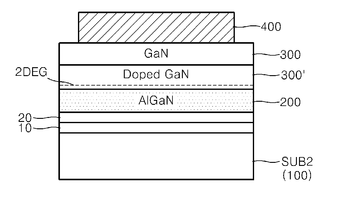
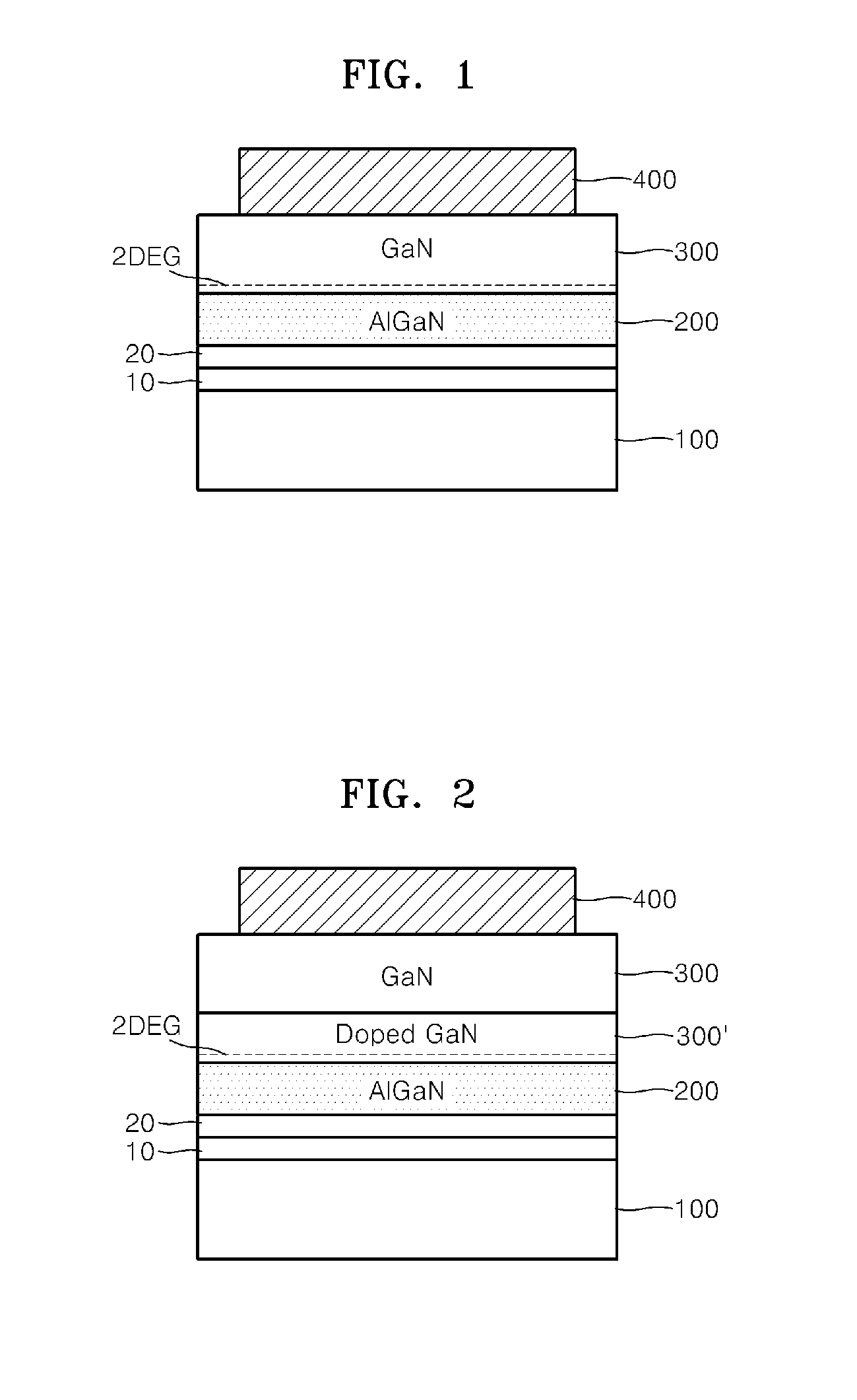
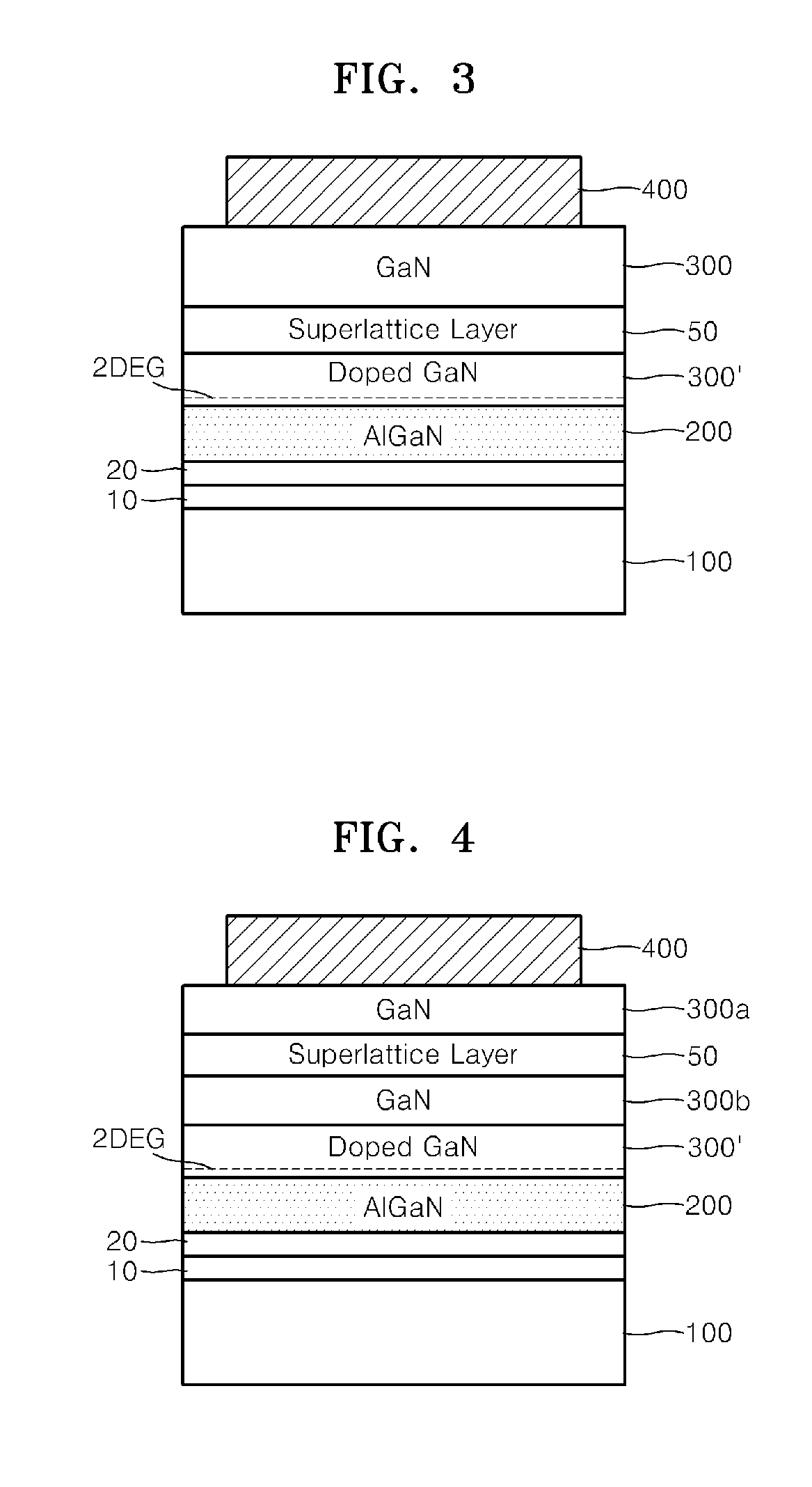
[0047]Various example embodiments will now be described more fully with reference to the accompanying drawings in which exemplary embodiments are shown.

[0048]It will be understood that when an element is referred to as being “connected” or “coupled” to another element, it can be directly connected or coupled to the other element or intervening elements may be present. In contrast, when an element is referred to as being “directly connected” or “directly coupled” to another element, there are no intervening elements present. As used herein the term “and / or” includes any and all combinations of one or more of the associated listed items.

[0049]It will be understood that, although the terms “first”, “second”, etc. may be used herein to describe various elements, components, regions, layers and / or sections, these elements, components, regions, layers and / or sections should not be limited by these terms. These terms are only used to distinguish one element, component, region, layer or sec...


PUM

PropertyMeasurementUnit
thicknessaaaaaaaaaa
thermal conductivityaaaaaaaaaa
structureaaaaaaaaaa

Abstract

Gallium nitride (GaN) based semiconductor devices and methods of manufacturing the same. The GaN-based semiconductor device may include a conductive heat dissipation substrate (that is, a thermal conductive substrate); an GaN-based multi-layer arranged on the heat dissipation substrate; and a Schottky electrode arranged on the GaN-based multi-layer. While such a GaN-based semiconductor device is being manufactured, a wafer bonding process and a laser lift-off process may be used.

Description

CROSS-REFERENCE TO RELATED PATENT APPLICATION[0001]This application claims the benefit of Korean Patent Application No. 10-2010-0093808, filed on Sep. 28, 2010, in the Korean Intellectual Property Office, the disclosure of which is incorporated herein in its entirety by reference.BACKGROUND[0002]1. Field[0003]The present disclosure relates to semiconductor devices and methods of manufacturing the same, and more particularly, to gallium nitride based semiconductor devices and methods of manufacturing the same.[0004]2. Description of the Related Art[0005]Recently, along with rapid developments in information and communication technologies, technologies for high-speed and massive-capacity signal transmission are being rapidly developed. In this regard, with an increasing demand for personal mobile phones, satellite communications, military radars, broadcasting communications, and communication relay devices, there has been an increasing request for high-speed and high-power electronic ...

Claims


Application Information

Patent Timeline
Patent Type & Authority Applications(United States)
IPC IPC(8): H01L33/32
CPCH01L21/2007H01L29/155H01L29/2003H01L29/872H01L29/66462H01L29/7787H01L29/66212H01L29/205
Inventor LEE, JAE-HOON
Owner SAMSUNG ELECTRONICS CO LTD
Why Eureka
Try Eureka