

Optical surface defect inspection apparatus and optical surface defect inspection method
a technology of optical surface defect and inspection apparatus, which is applied in the direction of optically investigating flaws/contamination, instruments, measurement devices, etc., can solve the problem that the autofocus operation cannot physically follow the scan rate, and achieve the effect of improving the signal-to-noise ratio and highly sensitive inspection
- Summary
- Abstract
- Description
- Claims
- Application Information
AI Technical Summary
Benefits of technology
Problems solved by technology
Method used
Image

Examples
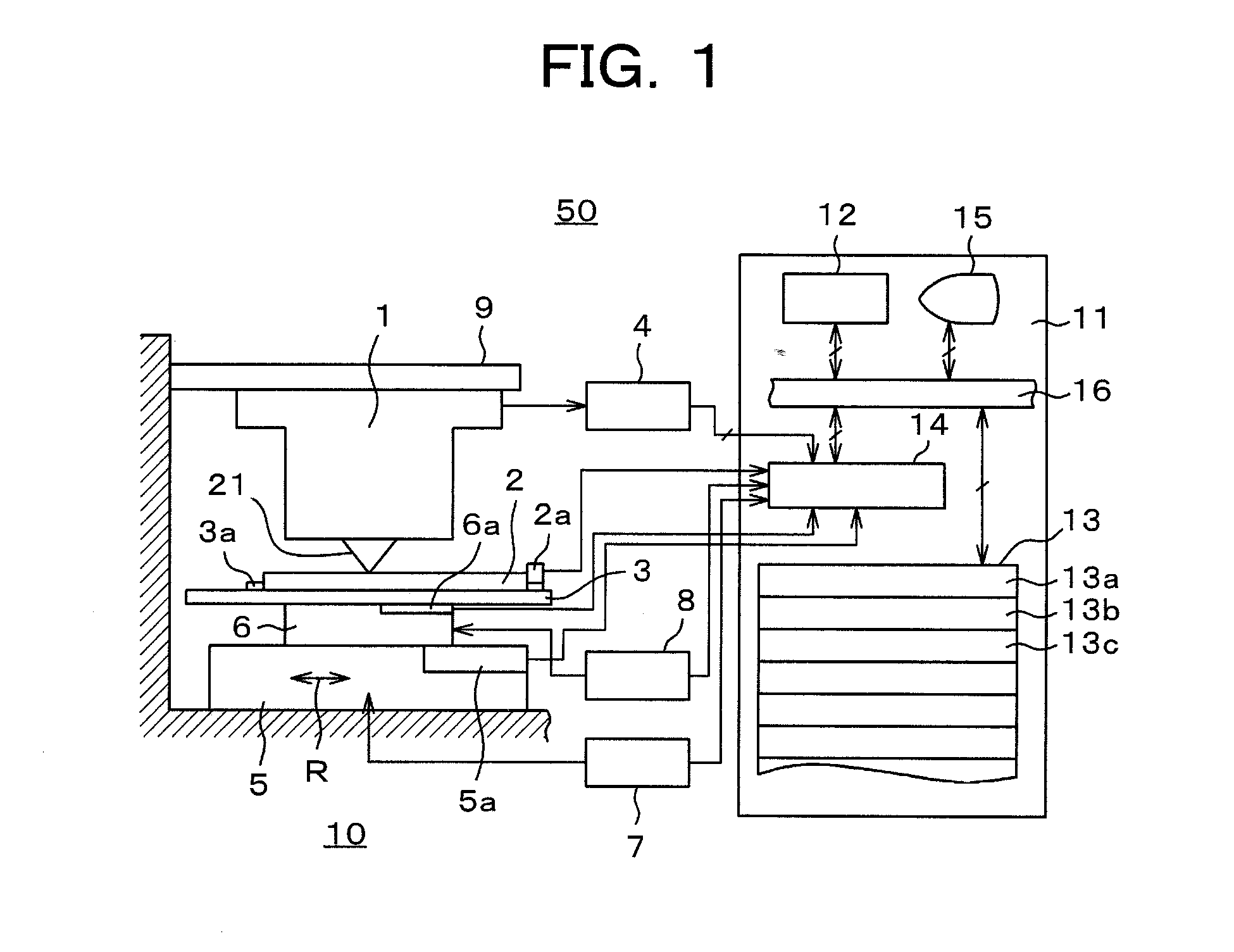
second embodiment
[0030]Of course, as shown in a second embodiment in FIG. 6, it is also possible to separately connect the individual cells A1 to H1 and A2 to H2 to light receiving devices 42A1 to 42H1 and 42A2 to 42H2. In this case, the number of cells divided in the light receiving surface may be an odd number.
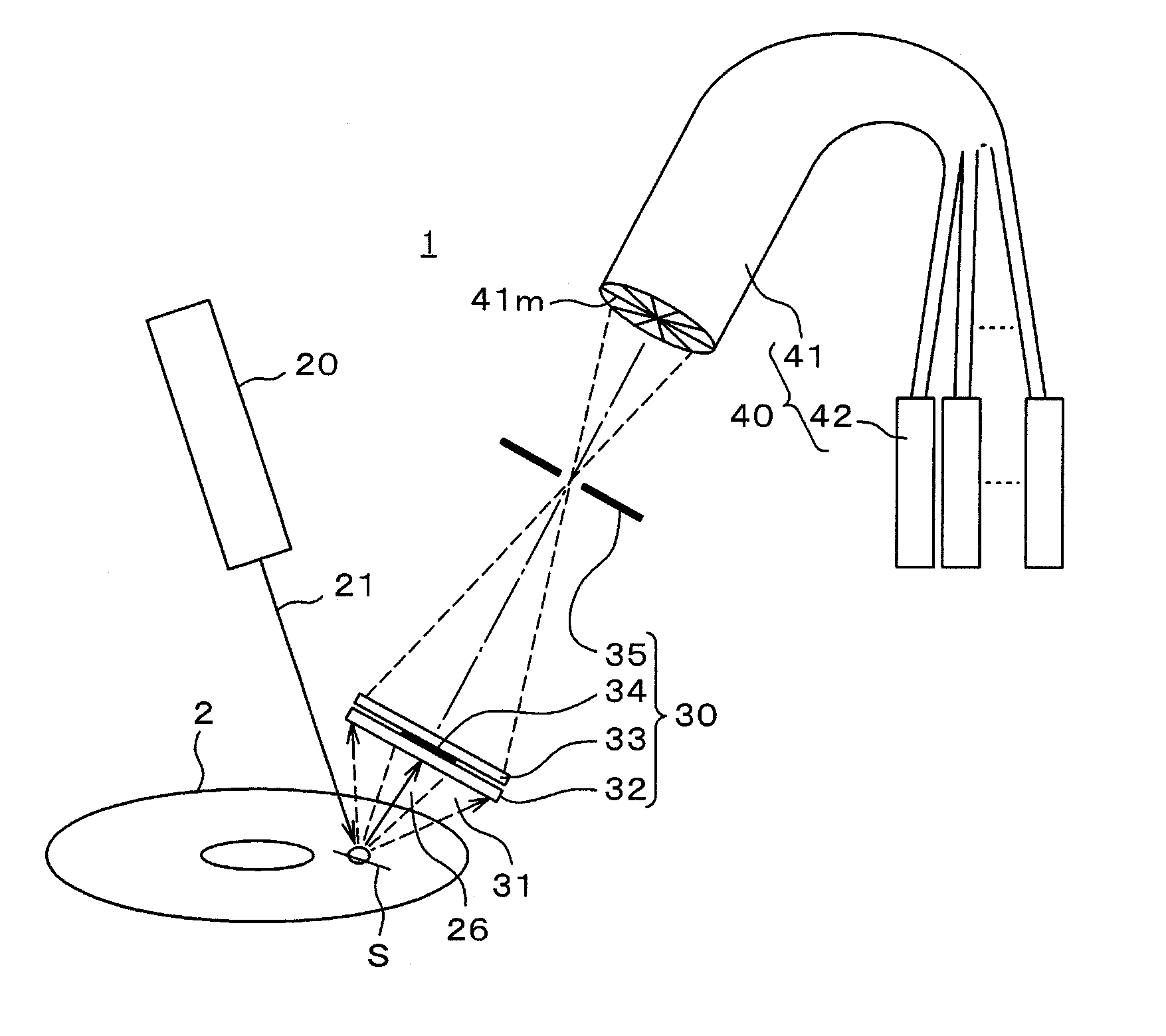
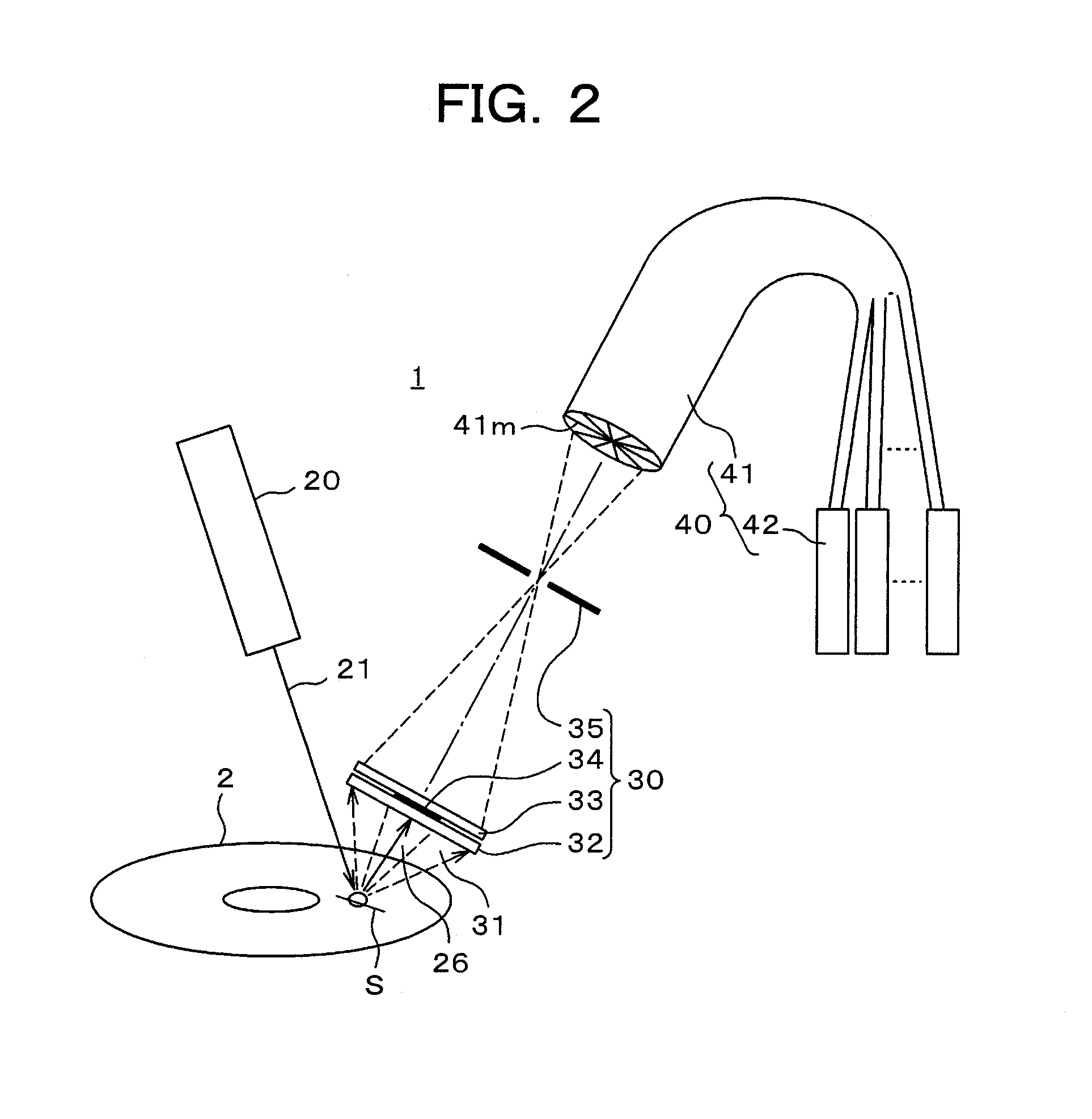
[0031]Next, the operation and effect of the inspection optical system 1 described above will be explained.
[0032]Generally, in the case where the surface of the test subject 2 is completely flat like a mirror, the scattered light 31 is rarely produced, and most of the reflected light becomes the positive reflected light 26. On the other hand, in the case where defects such as flaws exist on the surface of the test subject 2, a strong scattered light is produced. This change in the scattered light is captured to detect defects. Moreover, the intensity of scattered light is changed depending on the size or shape of defects.
first embodiment
[0033]When defects on the surface of the test subject are scratches and very shallow flaws, a scattered light to be produced is considerably weak, and it is difficult to distinguish between that scattered light and a scattered light that is background noise produced due to surface roughness or the like. Namely, it is difficult to detect the scattered light because the signal-to-noise ratio is low. For these shallow, scratch-like flaws, the embodiment can improve the signal-to-noise ratio and is effective. In the following, an example will be described in which the light receiving surface 41m is divided into 16 cells, which is an even number (2n), with reference to the first embodiment shown in FIGS. 3 and 5.
[0034]As described above, when the shape of a defect is a line-shaped scratch, such a characteristic is produced that a scattered light is distributed in the direction at a right angle to the orientation of this scratch. On the other hand, a scattered light (background noise) pro...
PUM
| Property | Measurement | Unit |
|---|---|---|
| length | aaaaa | aaaaa |
| center angle | aaaaa | aaaaa |
| angle | aaaaa | aaaaa |
Abstract
Description
Claims
Application Information