Semiconductor test device, semiconductor test circuit connection device, and semiconductor test method

a test circuit and semiconductor technology, applied in the direction of measurement devices, power supply testing, instruments, etc., can solve the problems of affecting the reliability of test equipment, so as to reduce the quantity of test contact devices, reduce equipment costs, and reduce initial investment

Active Publication Date: 2012-04-05
FUJI ELECTRIC CO LTD
View PDF4 Cites 22 Cited by
  • Summary
  • Abstract
  • Description
  • Claims
  • Application Information

AI Technical Summary

Benefits of technology

[0037]According to the semiconductor test device, semiconductor test circuit connection device, and semiconductor test method of the invention, it is possible to reduce the quantity of test contact devices by test functions being integrated. Also, it is possible to reduce initial investment, such as investment costs, and personnel costs. Furthermore, a sharing of tester components and measurement circuits is possible, and it is possible to reduce equipment costs.

Problems solved by technology

For this reason, when a large amount of space in a test device is taken up by the switch mechanism, it is difficult to dispose components, such as the inductor, required in the switching test circuit of FIG. 17.
Of the heretofore known test circuit configurations, it is necessary to connect an electrolytic capacitor, snubber circuit, test inductor, and the like, to the DUT for the switching test shown in FIG. 17 and the like, meaning that, as they have an effect on the DC characteristic measurement shown in FIG. 21, it is not possible to use the same contact device.
On the other hand, however, as the wiring in the test circuit as a whole is long, surge voltage (overvoltage) caused by wiring inductance when the DUT is turned off is liable to occur.
For this reason, a problem occurs in that measurement of characteristics such as rise time (tr) becomes difficult, or stress applied in an FWD reverse recovery test is insufficient.
This is because the stray inductance is a cause of surge voltage occurring during the test, and of the current change rate (di / dt), which is one test condition, becoming gentler, and causes a problem such as the voltage and current oscillating, damaging the DUT.
However, with this method of dealing with the matter, there are problems in that the quantity of each part increases, current measurement becomes complicated because it is necessary to cancel the current flowing through the snubber circuit in order to measure only the current flowing through the DUT, and the like.
Moreover, when the DUT is damaged, the whole of the charge stored in the capacitor connected to the P and N contact portions of the DUT flows from the capacitor into the DUT.
Because of this, when the capacity of the capacitor disposed in the immediate vicinity is large, the sound of explosion when the DUT is damaged is large, and there is a problem in that the state of damage to not only the DUT but also the peripheral circuit portion is noticeable.
In this way, when implementing an AC parametric test (switching test), AC parametric test (load short circuit test), thermal resistance test, and DC parametric test sequentially, heretofore, an independent tester and test contact device have been necessary for each test, and it has not been possible to use the same components or measurement circuits in each tester.
Because of this, the initial investment when introducing a semiconductor test device, that is, the equipment cost, increases.
Also, as the DUT needs to be loaded into and unloaded from a plurality of test contact devices, and moreover, time is needed to switch a mechanical switch, testing efficiency decreases, and personnel costs for implementing the tests also increase.
Furthermore, there is a problem such as that a conveying unit when conveying the DUT to the semiconductor test device is also complicated and expensive.

Method used


Image

  • Semiconductor test device, semiconductor test circuit connection device, and semiconductor test method
  • Semiconductor test device, semiconductor test circuit connection device, and semiconductor test method
  • Semiconductor test device, semiconductor test circuit connection device, and semiconductor test method

Examples


first embodiment

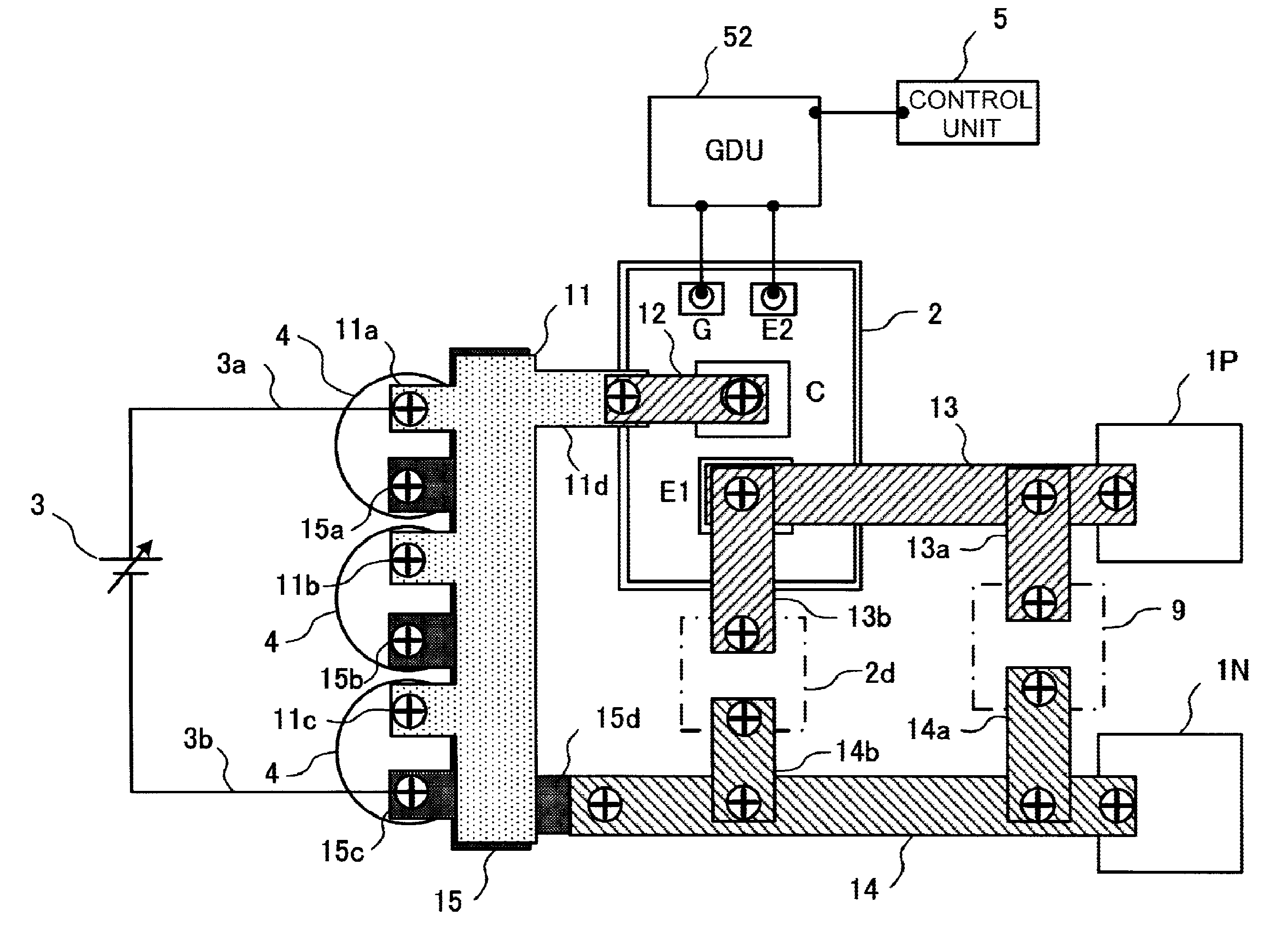
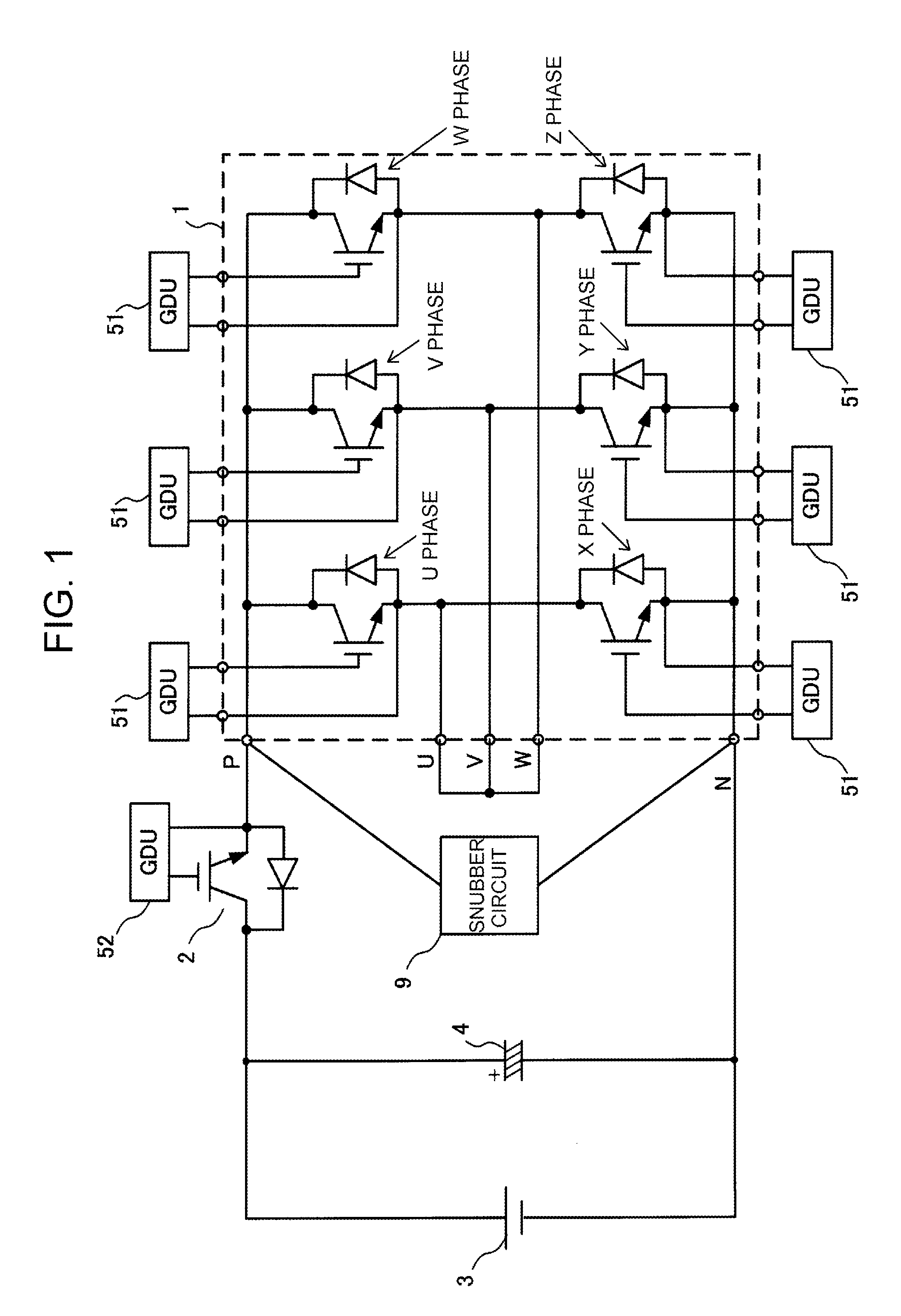
[0061]Firstly, a description will be given of an acceleration of a load short circuit test, which is one IGBT module AC parametric test. FIG. 1 is a circuit diagram showing a configuration of a test circuit for carrying out a load short circuit test at high speed.

[0062]A 6-in-1 type IGBT module 1 used when driving a three-phase alternating current motor is connected as a DUT in the test circuit. That is, a P terminal of the IGBT module 1 is connected to the positive side, and an N terminal to the negative side, of a DC power source, and output terminals (U, V, and W) are mutually short circuited in the immediate vicinity of the IGBT module 1. A DC power source 3 is connected between the P terminal and N terminal of the IGBT module 1 across a protective switch circuit 2. Also, an electrolytic capacitor 4 with a largish capacity is normally connected in parallel with the DC power source 3 in order to supply a charge sufficient to be able to carry a specified current from a power sourc...

second embodiment

[0071]Next, a description will be given of a test circuit that implements a switching test, which is another AC parametric test, integrally with a load short circuit test.

[0072]FIG. 3 is a circuit diagram showing a configuration of an integrated test circuit for integrally implementing a switching test and load short circuit test.

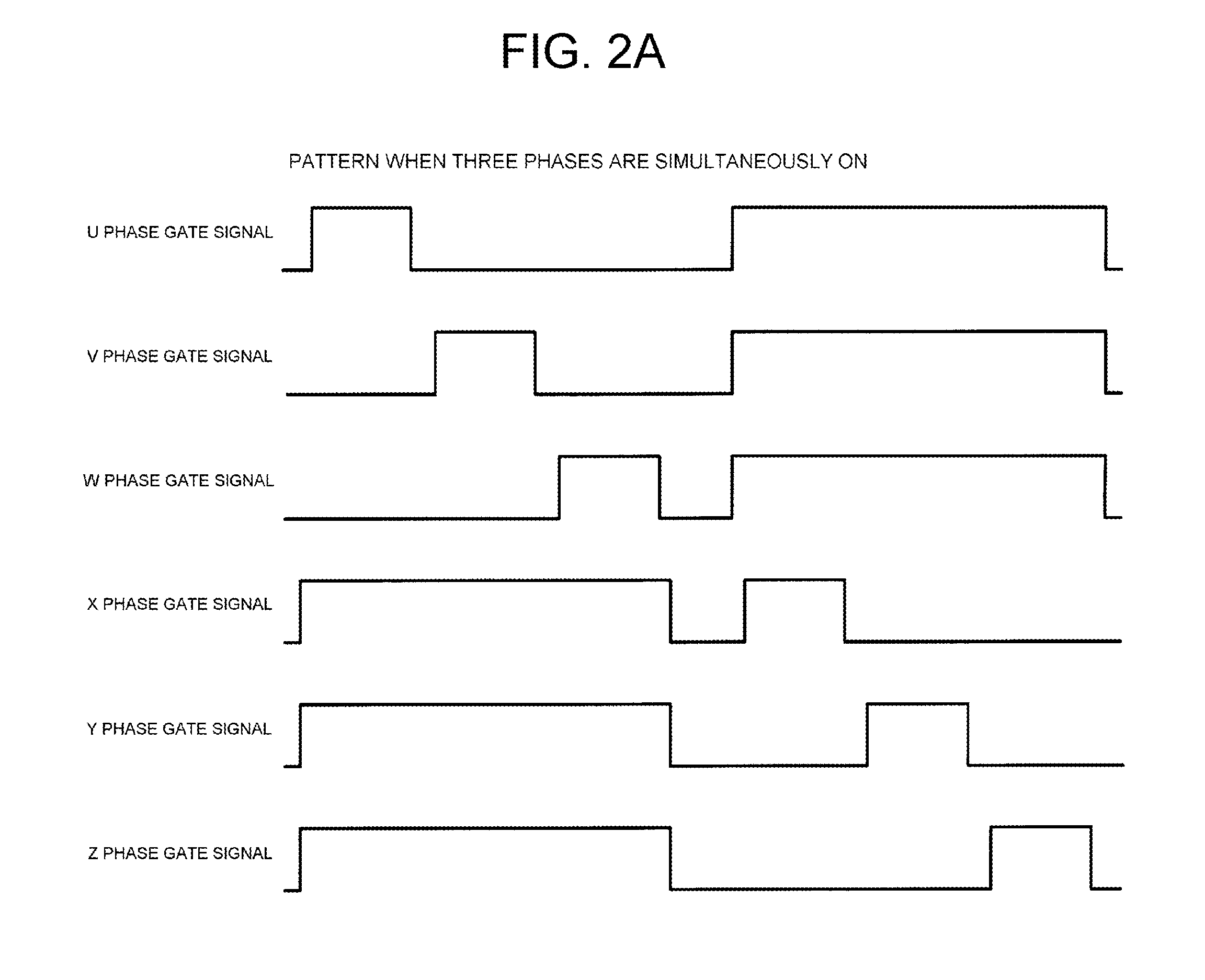
[0073]In the integrated test circuit too, with the 6-in-1 type IGBT module 1 as the DUT, the P terminal of the DUT is connected to the positive side, and the N terminal to the negative side, of the DC power source 3. Also, a load inductor 6 is connected to each of the output terminals (U, V, and W) in a star connection, and switches SW11 and SW12, which cause a short circuit between the output terminals, are connected in parallel with the load inductor 6. Although there is no switch in the wire from the V terminal in FIG. 3, a switch may be inserted. Furthermore, the gate drive units 51 are connected individually to the gate terminal and auxiliary emitter t...

third embodiment

[0079]FIG. 5 is a circuit diagram showing a configuration of a test circuit for integrally implementing a DC parametric test and AC parametric test, and FIG. 6 is a side view showing the structure of a DC / AC integrated tester for realizing the test circuit of FIG. 5.

[0080]With this test circuit, it is possible to sequentially implement a DC parametric test, including also a thermal resistance test, and AC parametric tests (switching test and load short circuit test) using the same contact device, with the 6-in-1 type IGBT module 1 as the DUT, by setting a change between a heretofore known DC test circuit shown in FIG. 21 and the AC test circuit shown in FIG. 3 by switching with a switch.

[0081]A plurality of switches that can be turned on and off are shown in FIG. 5. Also, only a force line is shown as a connecting line from each terminal (positioned at the intersections of the broken line and circle symbols) of the IGBT module 1 to a DC tester 17. Actually, however, a sense line fro...


PUM


Abstract

A semiconductor test device and method for sequentially carrying out tests including an AC test, DC test, and thermal resistance test on a power semiconductor device are provided. The semiconductor test device includes a holding unit that positions the power semiconductor device. Test units each generate a test signal for the power semiconductor device and determine a test result generated in response to the test signal. A connection unit switches between the test units and selectively connects the test units electrically to electrodes of the power semiconductor device. The connection unit is controlled such that the test units are sequentially connected to the power semiconductor device to perform a plurality of the tests. The connection unit may include parallel plate electrodes in proximity to each other across an insulating sheet. The parallel plate electrodes may connect the power semiconductor device to positive and negative power sources of the test unit.

Description

CROSS-REFERENCE TO RELATED APPLICATION[0001]This application claims the benefit of priority of Japanese patent application number 2010-222788, filed on Sep. 30, 2010, the disclosure of which is incorporated herein by reference.BACKGROUND OF THE INVENTION[0002]1. Technical Field[0003]The present invention relates to a semiconductor test device, semiconductor test circuit connection device, and semiconductor test method that enable various kinds of semiconductor device test to be integrally carried out, and relates in particular to a rationalization of a power semiconductor module test method, an improvement of testing conditions (waveform), and a semiconductor test device improved thereby.[0004]2. Related Art[0005]Final tests and various kinds of test during the manufacturing process on power semiconductor products typified by an insulated gate bipolar transistor (IGBT), a power metal oxide semiconductor field effect transistor (MOSFET), or the like, are broadly divided into a therma...

Claims


Application Information

Patent Timeline
Patent Type & Authority Applications(United States)
IPC IPC(8): G01R31/26
CPCG01R31/2608G01R31/42G01R31/2841G01R31/2628
Inventor YOSHIDA, ATSUSHI
Owner FUJI ELECTRIC CO LTD
Why Eureka
Try Eureka