Light-emitting diode device and manufacturing method thereof

a technology of light-emitting diodes and manufacturing methods, which is applied in the direction of semiconductor/solid-state device manufacturing, semiconductor devices, electrical devices, etc., can solve the problems of easy consumption of device b>1/b> at the interface, reduced output of light, and easy etching of devices, etc., to shorten the manufacturing period, reduce light consumption, and improve the effect of etching efficiency

Inactive Publication Date: 2012-04-12
CHI MEI LIGHTING TECH
View PDF5 Cites 14 Cited by
  • Summary
  • Abstract
  • Description
  • Claims
  • Application Information

AI Technical Summary

Benefits of technology

[0019]In one embodiment, the depression is formed by wet etching or the combination of wet etching and laser illumination. Laser illumination causes the separation of the substrate and the epitaxial layer, facilitating the lateral etching with the etchant to enhance the etching efficiency.
[0020]As mentioned above, a depression is formed on the sidewall of the LED device and a reflective layer is formed on the depression in the invention, so the light generated by the LED device can be reflected through the reflective layer, resulting in decreasing the light consumption occurred at the interface of the substrate and the epitaxial layer and the light absorbed by the substrate, and adjusting the light-emitting direction of the LED device. Besides, because the light-emitting direction can be adjusted by the LED device itself, the LED device is favorable for the compactness with a shortened manufacturing period, and thus the production competitiveness can be enhanced.

Problems solved by technology

However, due to mismatch of refraction indexes of the substrate 11 and the epitaxial layer, the light generated by the LED device 1 is easily consumed at the interface, and the output of the light is thus decreased.
However, this not only increases the steps of manufacturing but also is unfavorable to the compactness.

Method used


Image

  • Light-emitting diode device and manufacturing method thereof
  • Light-emitting diode device and manufacturing method thereof
  • Light-emitting diode device and manufacturing method thereof

Examples


Embodiment Construction

[0028]The present invention will be apparent from the following detailed description, which proceeds with reference to the accompanying drawings, wherein the same references relate to the same elements.

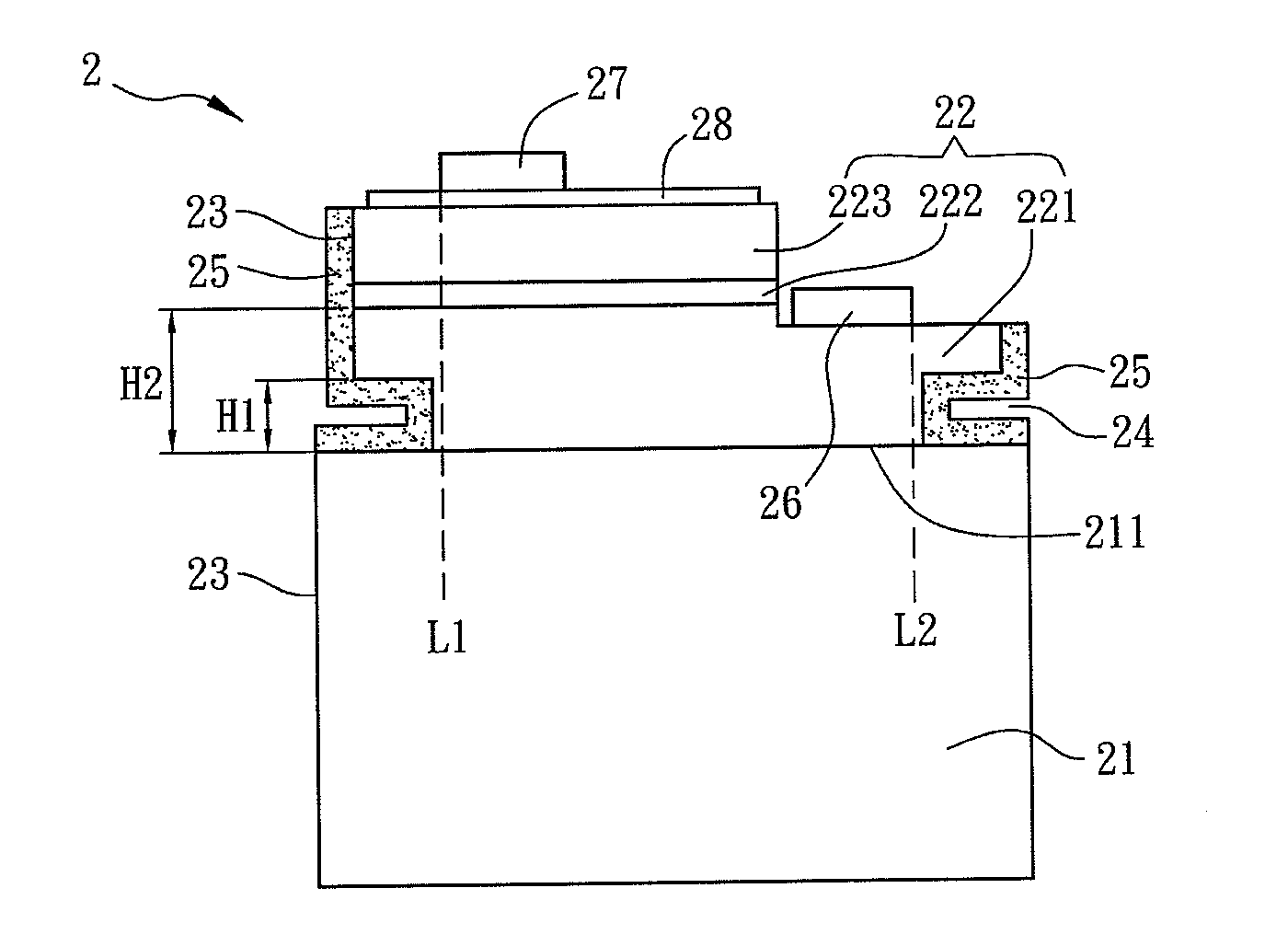
[0029]FIG. 2 is a schematic diagram of a light-emitting diode (LED) device 2 of a preferred embodiment of the invention. As shown in FIG. 2, the LED device 2 includes a substrate 21 and an epitaxial layer 22 which is disposed on a surface 211 of the substrate 21. Besides, a depression 24 is disposed on a sidewall 23 of the LED device 2, and a reflective layer 25 is disposed to on least one portion of the depression 24.

[0030]The material of the substrate 21 is not limited in the embodiment, which can include, for example, sapphire, SiC, GaP or Si. Here, the substrate 21 is made of sapphire for example.

[0031]The epitaxial layer 22 is disposed on the substrate 21. The epitaxial layer 22 is a semiconductor layer formed by epitaxy technology, including a first conductivity type semiconduct...


PUM


Abstract

A light-emitting diode (LED) device includes a substrate and an epitaxial layer which is disposed on a surface of the substrate. A depression is disposed to a sidewall of the LED device, and a reflective layer is disposed to on least one portion of the depression. By the reflective layer disposed to the depression of the sidewall of the LED device, the light loss caused by the interface of the substrate and the epitaxial layer can be reduced, the light absorbed by the substrate can be decreased, and the angle of the light exiting from the LED device can be adjusted. A manufacturing method of the LED device is also disclosed.

Description

CROSS REFERENCE TO RELATED APPLICATIONS[0001]This Non-provisional application claims priority under 35 U.S.C. §119(a) on Patent Application No(s). 099134107 filed in Republic of China on Oct. 6, 2010, the entire contents of which are hereby incorporated by reference.BACKGROUND OF THE INVENTION[0002]1. Field of Invention[0003]The invention relates to a light-emitting diode device and a manufacturing method thereof and, in particular, to a light-emitting diode device having a reflecting layer disposed on a sidewall thereof.[0004]2. Related Art[0005]Light-emitting diodes (LED), made of semiconductor material, have advantages such as low power consumption, long lifespan, and fast response. In addition, since the LEDs can be easily manufactured to a small device or an array device, they are widely applied to various appliances, such as indicators of the computers or the household appliances, backlights of the LCD apparatuses, traffic lights and vehicle lights.[0006]FIG. 1 is a schematic ...

Claims


Application Information

Patent Timeline
Patent Type & Authority Applications(United States)
IPC IPC(8): H01L33/46
CPCH01L33/20H01L2933/0025H01L33/46
Inventor YU, KUO-HUICHU, CHANG-HSIN
Owner CHI MEI LIGHTING TECH
Why Eureka
Try Eureka