Semiconductor structure and method for making the same

a semiconductor and structure technology, applied in the direction of semiconductor devices, semiconductor/solid-state device details, electrical apparatus, etc., can solve the problems of reducing the operational performance of the desired semiconductor elements, and reducing the total electric resistance, so as to reduce the critical dimension, avoid adverse effects, and increase current

Inactive Publication Date: 2012-04-12
UNITED MICROELECTRONICS CORP
View PDF4 Cites 24 Cited by
  • Summary
  • Abstract
  • Description
  • Claims
  • Application Information

AI Technical Summary

Benefits of technology

[0009]Accordingly, the present invention proposes a novel semiconductor structure. This novel semiconductor structure not only supports a larger current but also avoids some adverse consequences. In this way, problems such as overly decreased critical dimension, the extreme intrinsic resistance within the source contact plugs and drain contact plugs and deteriorated operational performance of the semiconductor elements can be thoroughly solved.
[0010]The present invention in a first aspect proposes a semiconductor structure. The semiconductor structure of the present invention includes a substrate, a gate structure, a source, a drain, a source contact plug and a drain contact plug. The gate structure is disposed on the substrate. The source and the drain are respectively disposed in the substrate at two sides of the gate structure. The source contact plug is disposed above the source and electrically connected to the source. The drain contact plug is disposed above the drain and electrically connected to the drain. One feature of the present invention resides in the relatively asymmetric element properties of the source contact plug and the drain contact plug so that the electric resistance of the source contact plug or the drain contact plug can be decreased. The element property may be at least one of a shape, a size, a material, a stress, an aspect ratio and a quantity.
[0011]The present invention in a second aspect proposes a semiconductor structure. The semiconductor structure of the present invention includes a substrate, a gate structure, a source, a drain, a source contact plug and a drain contact plug. The gate structure is disposed on the substrate. The source and the drain are respectively disposed in the substrate at two sides of the gate structure. The source contact plug is disposed above the source and electrically connected to the source. The drain contact plug is disposed above the drain and electrically connected to the drain. Another feature of the present invention resides in the relatively asymmetric element properties of the source contact plug and the drain contact plug so that the capacitor effect of the source contact plug or the drain contact plug on the gate structure can be decreased. The element property may be at least one of a shape, a size, a material, a stress, an aspect ratio, a quantity and a distance to the gate structure. Preferably, the capacitor effect of the source contact plug on the gate structure is larger than that of the drain contact plug on the gate structure.

Problems solved by technology

However, with the trend of pursuing elements to be as small as possible, the intrinsic resistance within the source contact plugs and drain contact plugs due to the overly decreased critical dimension becomes too large to support the current to maintain a normal on and off state, which jeopardizes the desirable operational performance of the semiconductor elements.
Albeit the slot layout structure seemingly reduces the total electric resistance to be able to support a larger current, serious sequels to this happen.
For example, the slot structure may have serious and adverse interactions such as coupling with the gate structure.
In such a way, the operational performance of the semiconductor elements does not improve at all.

Method used


Image

  • Semiconductor structure and method for making the same
  • Semiconductor structure and method for making the same
  • Semiconductor structure and method for making the same

Examples


Embodiment Construction

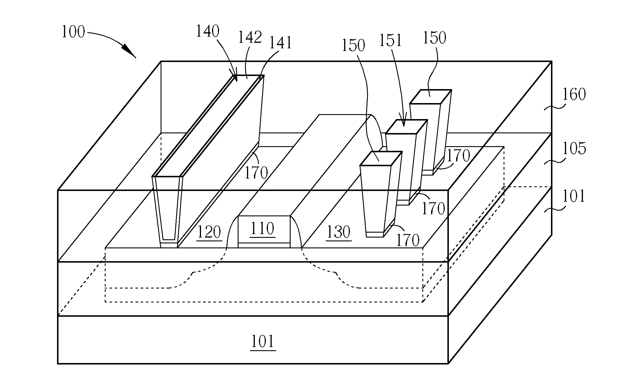
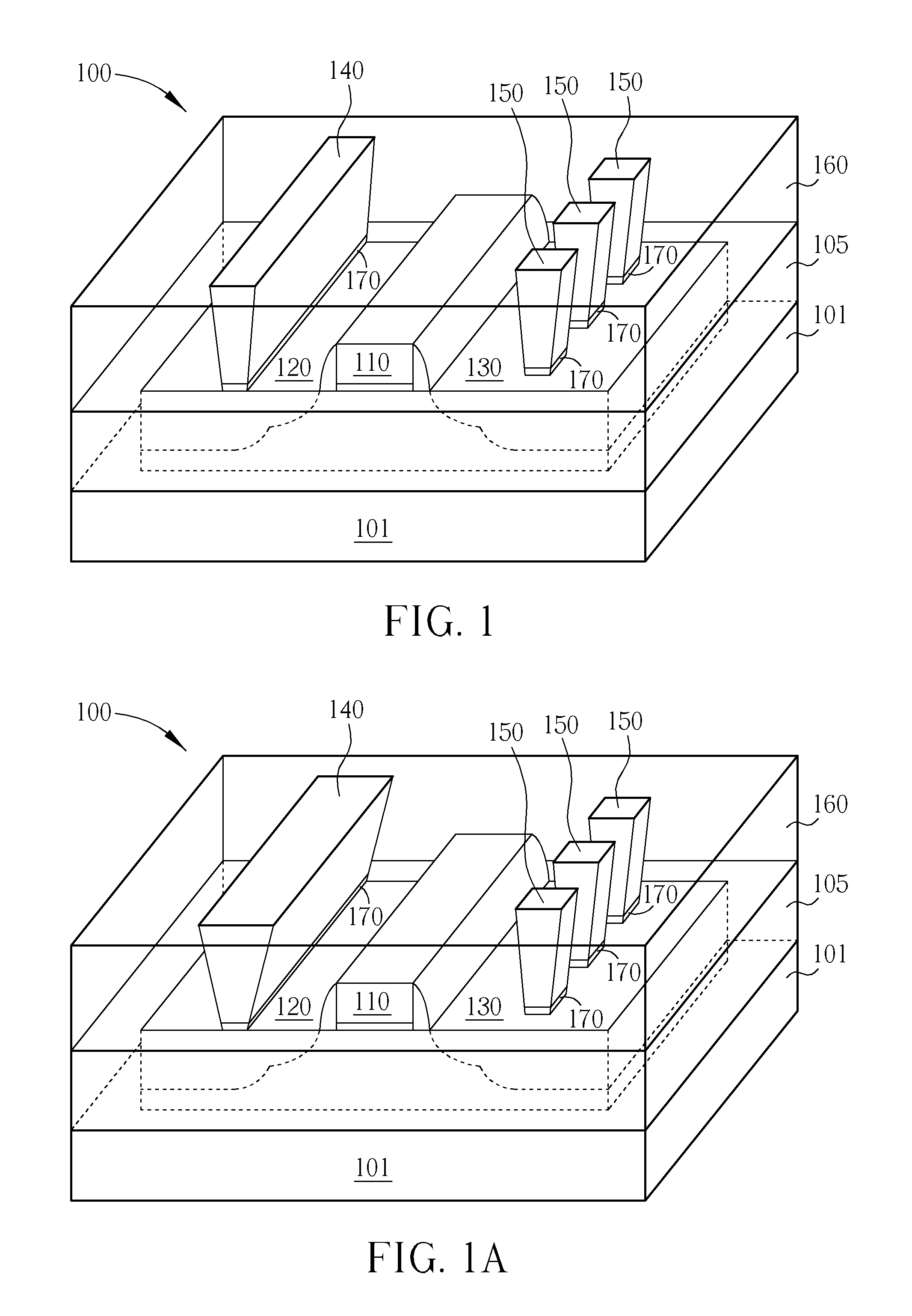
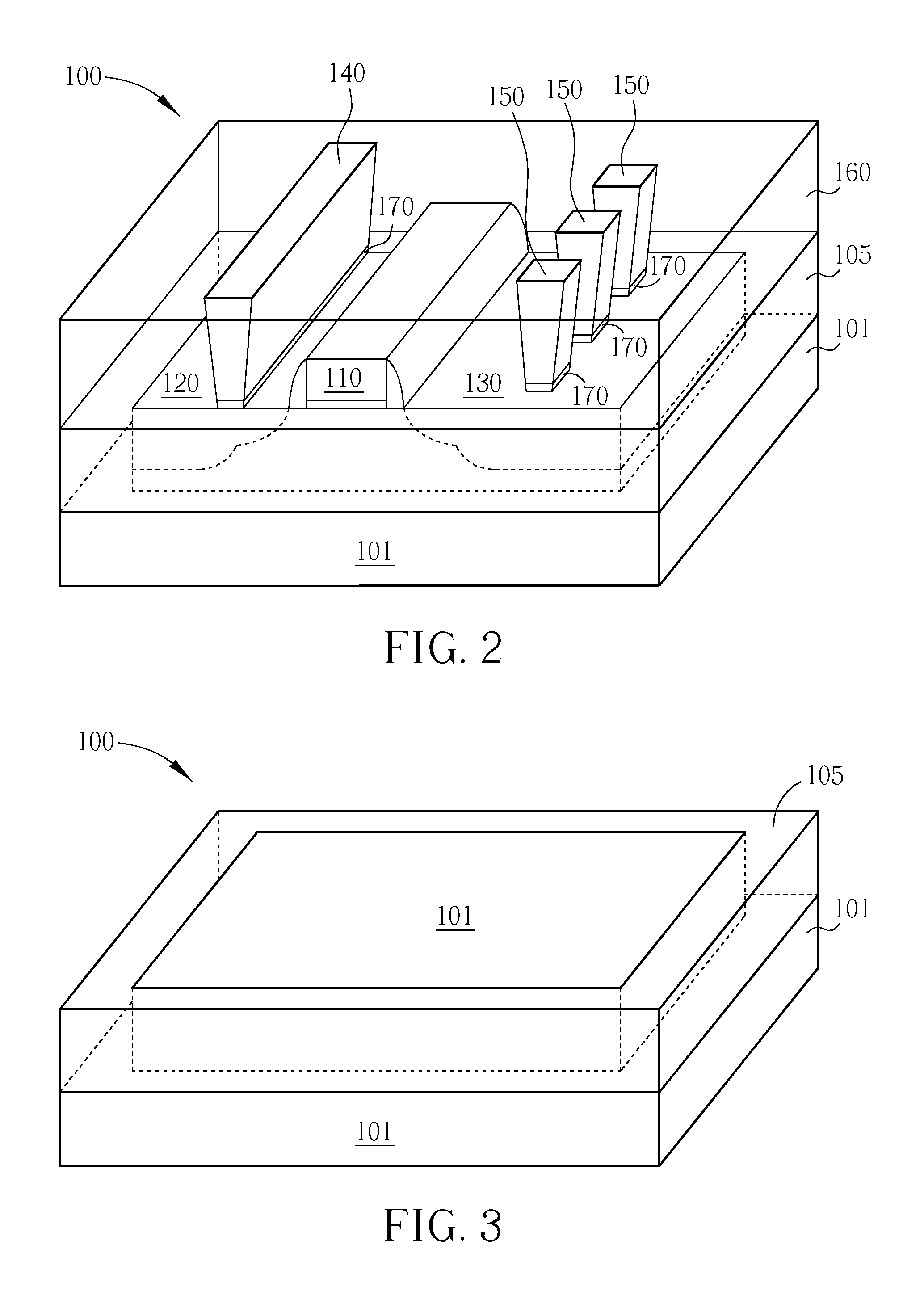
[0018]The present invention provides a novel semiconductor structure. The source contact plug and the drain contact plug in the light of each individual semiconductor element have at least one relatively asymmetric element property so that the element properties of the source contact plug or the drain contact plug can be independently adjusted. As a result, the capacitor effect of the source contact plug or of the drain contact plug on an individual gate structure, or the electric resistance of the source contact plug or the drain contact plug can be properly adjusted. The novel semiconductor structure of the present invention accordingly allows a larger operational current, or exhibits less capacitor to an individual gate structure to maintain an optimal performance of the semiconductor element.

[0019]The present invention in a first aspect provides a novel semiconductor structure. FIG. 1 illustrates a perspective view of the semiconductor structure of the present invention. Please ...


PUM


Abstract

A semiconductor structure is disclosed. The semiconductor structure includes a gate structure disposed on a substrate, a source and a drain respectively disposed in the substrate at two sides of the gate structure, a source contact plug disposed above the source and electrically connected to the source and a drain contact plug disposed above the drain and electrically connected to the drain. The source contact plug and the drain contact plug have relatively asymmetric element properties.

Description

BACKGROUND OF THE INVENTION[0001]1. Field of the Invention[0002]The present invention generally relates to a semiconductor structure and the method for making the same. In particular, the present invention is directed to a semiconductor structure whose source contact plug and drain contact plug have relatively asymmetric element properties as well as a method for fabricating a semiconductor structure.[0003]2. Description of the Prior Art[0004]In a regular semiconductor structure, a gate structure is used to control the on and off state of a current passing through the source and the drain which are disposed at two sides of the gate structure. Because the source and the drain are respectively disposed in the substrate at two sides of the gate structure and covered by an interlayer dielectric layer, a source contact plug and a drain contact plug are still needed to respectively penetrate the interlayer dielectric layer to form an electrical connection of the source and the drain to an...

Claims


Application Information

Patent Timeline
Patent Type & Authority Applications(United States)
IPC IPC(8): H01L29/78H01L21/336
CPCH01L23/485H01L29/7833H01L29/7843H01L2924/0002H01L2924/00
Inventor CHENG, TZYY-MINGTSAI, MENG-CHICHEN, TSAI-FULO, TA-KANGHUNG, WEN-HANTZOU, SHIH-FANGWU, CHUN-YUAN
Owner UNITED MICROELECTRONICS CORP
Why Eureka
Try Eureka