Wavelength conversion component

a technology of wavelength conversion and component, which is applied in the direction of discharge tube luminescnet screens, fixed installations, lighting and heating apparatus, etc., can solve the problems of loss of sales to target customers, variation in the color of emitted light with emission angle, and non-white color appearance of devices in off-state, so as to improve the color uniformity of emitted light, and reduce the quantity of phosphor material

Active Publication Date: 2012-04-12
FEIT ELECTRIC CO INC
View PDF6 Cites 56 Cited by
  • Summary
  • Abstract
  • Description
  • Claims
  • Application Information

AI Technical Summary

Benefits of technology

[0011]One benefit of this approach is that by selecting an appropriate particle size and concentration per unit area of the light diffractive material, an improvement is obtained in the white color appearance of a LED device in its OFF state. Another benefit is an improvement to the color uniformity of emitted light from an LED device for emission angles over a ±60° range from the emission axis. Moreover the use of a light diffusing layer having an appropriate particle size and concentration per unit area of the light diffractive material can substantially reduce the quantity of phosphor material required to generate a selected color of emitted light, since the light diffusing layer increases the probability that a photon will result in the generation of photoluminescence light by directing light back into the wavelength conversion layer. Therefore, inclusion of a diffusing layer in direct contact with the wavelength conversion layer can reduce the quantity of phosphor material required to generate a given color emission product, e.g., by up to 40%. In one embodiment the particle size of the light diffractive material is selected such that excitation radiation generated by the source is scattered more than light generated by the one or more phosphor materials.
[0012]According to some embodiments of the invention a wavelength conversion component for a light emitting device comprising at least one light emitting solid-state radiation source, comprises a light transmissive substrate having a wavelength conversion layer comprising particles of at least one photoluminescence material and a light diffusing layer comprising particles of a light diffractive material; and wherein the layers are in direct contact with each other. Preferably the wavelength conversion layer comprises a mixture of at least one phosphor material and a light transmissive binder while the light diffusing layer comprises a mixture of the light diffractive material and a light transmissive binder. To minimize optical losses at the interface of the layers it is preferred that the layers comprise the same transmissive binder. The binder can comprise a curable liquid polymer such as a polymer resin, a monomer resin, an acrylic, an epoxy, a silicone or a fluorinated polymer. The binder is preferably UV or thermally curable.
[0013]To reduce the variation in emitted light color with emission angle the weight loading of light diffractive material to binder is in a range 7% to 35% and more preferably in a range 10% to 20%. The wavelength conversion and light diffusing layers are preferably deposited by screen printing though they can be deposited using other deposition techniques such as spin coating or doctor blading. The light diffractive material preferably comprises titanium dioxide (TiO2) though it can comprise other materials such as barium sulfate (BaSO4), magnesium oxide (MgO), silicon dioxide (SiO2) or aluminum oxide (Al2O3).
[0014]In one arrangement the light diffractive material has an average particle size in a range 1 μm to 50 μm and more preferably in a range 10 μm to 20 μm. In other arrangements the light diffractive material has a particle size that is selected such that the particles will scatter excitation radiation relatively more than they will scatter light generated by the at least one photoluminescence material. For example, for blue light radiation sources, the light diffractive particle size can be selected such that the particles will scatter blue light relatively at least twice as much as they will scatter light generated by the at least one phosphor material. Such a light diffusing layer ensures that a higher proportion of the blue light emitted from the wavelength conversion layer will be scattered and directed by the light diffractive material back into the wavelength conversion layer increasing the probability of the photon interacting with a phosphor material particle and resulting in the generation of photoluminescent light. At the same time, phosphor generated light can pass through the diffusing layer with a lower probability of being scattered. Since the diffusing layer increases the probability of blue photons interacting with a phosphor material particle, less phosphor material can be used to generate a selected emission color. Such an arrangement can also increase luminous efficacy of the wavelength conversion component / device. Preferably the light diffractive material has an average particle size of less than about 150 nm where the excitation radiation comprises blue light. When the excitation radiation comprises UV light, the light diffractive material may have an average particle size of less than about 100 nm.

Problems solved by technology

One issue with remote phosphor devices is the non-white color appearance of the device in its OFF state.
This may be off-putting or undesirable to the potential purchasers and hence cause loss of sales to target customers.
Another problem with remote phosphor devices can be the variation in color of emitted light with emission angle.
In particular, such devices are subject to perceptible non-uniformity in color when viewed from different angles.
Such visually distinctive color differences are unacceptable for many commercial uses, particularly for the high-end lighting that often employ LED lighting devices.
Yet another problem with using phosphor materials is that they are relatively costly, and hence correspond to a significant portion of the costs for producing phosphor-based LED devices.
This results in a relatively small layer of phosphor materials placed directly on the LED die, that is nevertheless still costly to produce in part because of the significant costs of the phosphor materials.
As a result, the costs are correspondingly greater as well to provide the increased amount of phosphor materials needed for such remote phosphor LED devices.

Method used


Image

  • Wavelength conversion component
  • Wavelength conversion component
  • Wavelength conversion component

Examples


Embodiment Construction

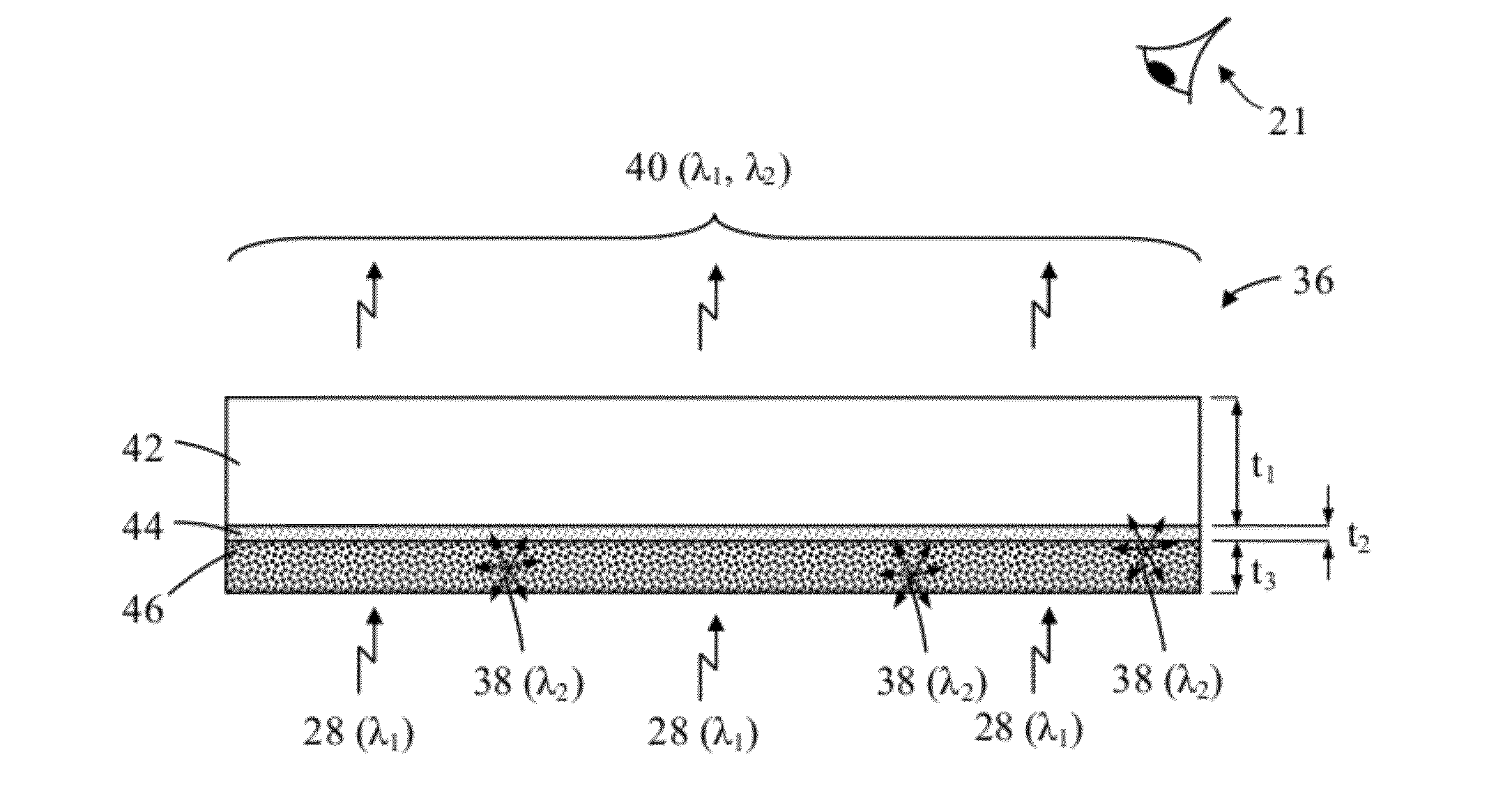
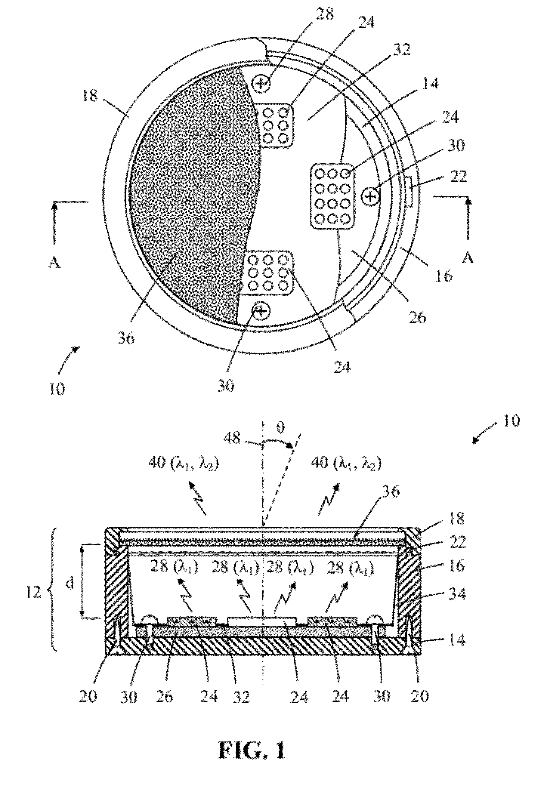
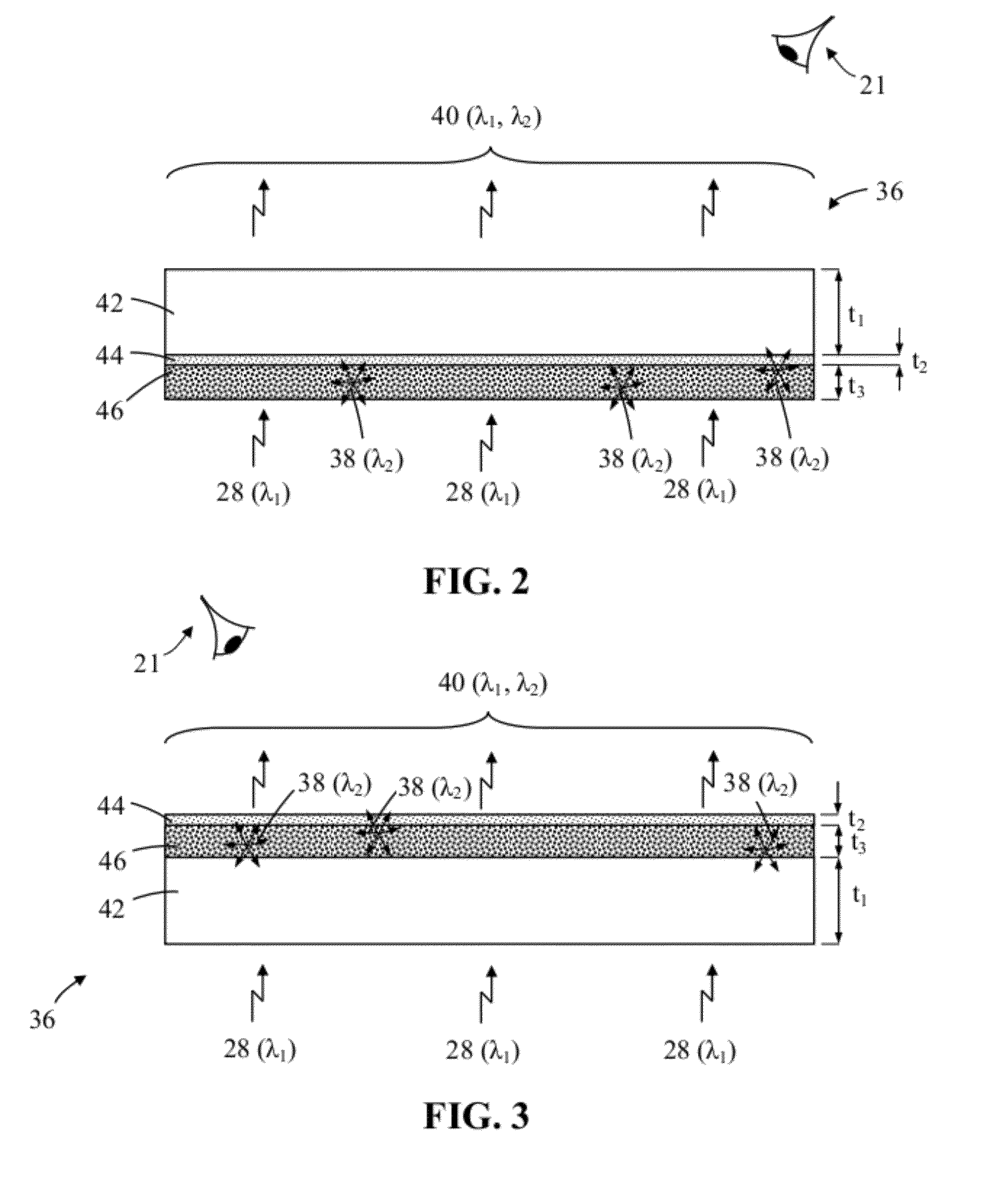
[0043]Some embodiments of the invention are directed to light emitting devices comprising one or more solid-state light emitters, typically LEDs, that is / are operable to generate excitation light (typically blue or UV) which is used to excite a wavelength conversion component containing particles of a photoluminescence materials (e.g. phosphor materials), such as a blue light excitable phosphor material or an UV excitable phosphor material. Additionally the wavelength conversion component comprises a light diffusing layer comprising particles of a light diffractive material (also referred to herein as “light scattering material”). One benefit of this arrangement is that by selecting an appropriate particle size and concentration per unit area of the light diffractive material, it is possible to make a device having an emission product color that is virtually uniform with emission angle over a ±60° range from the emission axis. Moreover the use of a light diffusing layer can substant...


PUM

PropertyMeasurementUnit
particle sizeaaaaaaaaaa

Abstract

A light emitting device comprises at least one solid-state light source (LED) operable to generate excitation light and a wavelength conversion component located remotely to the at least one source and operable to convert at least a portion of the excitation light to light of a different wavelength. The wavelength conversion component comprises a light transmissive substrate having a wavelength conversion layer comprising particles of at least one photoluminescence material and a light diffusing layer comprising particles of a light diffractive material. This approach of using the light diffusing layer in combination with the wavelength conversion layer solves the problem of variations or non-uniformities in the color of emitted light with emission angle. In addition, the color appearance of the lighting apparatus in its OFF state can be improved by implementing the light diffusing layer in combination with the wavelength conversion layer. Moreover, significant reductions can be achieved in the amount phosphor materials required to implement phosphor-based LED devices.

Description

CROSS-REFERENCE TO RELATED APPLICATIONS[0001]This application claims the benefit of priority to U.S. Provisional Patent Application Ser. No. 61 / 427,411, entitled “Solid-State Light Emitting Devices with Remote Phosphor Wavelength Conversion Component”, filed Dec. 27, 2010, which is hereby incorporated by reference in its entirety. This application is also a continuation-in-part of U.S. application Ser. No. 13 / 253,031, entitled “Solid-State Light Emitting Devices and Signage with Photoluminescence Wavelength Conversion,” filed on Oct. 4, 2011, which claims the benefit of U.S. Provisional Patent Application Ser. No. 61 / 390,091, entitled “Solid-State Light Emitting Devices and Signage with Photoluminescence Wavelength Conversion,” filed on Oct. 5, 2010, which is hereby incorporated by reference in its entirety.FIELD[0002]This disclosure relates to solid-state light emitting devices that use a remotely positioned phosphor wavelength conversion component to generate a desired color of li...

Claims


Application Information

Patent Timeline
Patent Type & Authority Applications(United States)
IPC IPC(8): F21V9/16
CPCF21K9/135F21V29/74F21K9/56F21S8/02F21V3/00F21V3/0481F21V9/16F21Y2101/02F21Y2105/001H01L33/50H01L2933/0091H01L2924/0002F21K9/17H01L2924/00F21K9/232F21K9/27F21K9/64F21V3/061F21V3/062F21V3/12F21V9/32F21V13/08F21Y2105/16F21Y2105/18F21Y2115/10F21Y2115/30
Inventor DAI, BINGYUAN, XIANGLONGWANG, GANGEDWARDS, CHARLESCARUSO, JAMES
Owner FEIT ELECTRIC CO INC
Why Eureka
Try Eureka