Limiting strain relaxation in iii-nitride hetero-structures by substrate and epitaxial layer patterning

a technology of iiiinitride and hetero-structure, which is applied in the direction of semiconductor devices, lasers, semiconductor lasers, etc., can solve the problems of limiting the design space of devices, affecting the performance of lds, and unable to fully realize the expected inherent advantages of device manufacturers, etc., and achieves the effect of higher alloy composition

Active Publication Date: 2012-04-26
RGT UNIV OF CALIFORNIA
View PDF1 Cites 13 Cited by
  • Summary
  • Abstract
  • Description
  • Claims
  • Application Information

AI Technical Summary

Benefits of technology

[0015]One or more of the semipolar or nonpolar III-nitride device layers can be thicker, and have a higher alloy composition, as compared to (1) semi-polar or nonpolar III-nitride device layers that are grown on a non-patterned surface of a semi-polar or nonpolar III-nitride substrate or epilayer, or as compared to (2) semi-polar or nonpolar III-nitride device layers that are grown on a different patterned surface of the semipolar or nonpolar III-nitride substrate.

Problems solved by technology

In spite of numerous advantages offered by growth of optoelectronic devices on nonpolar / semipolar III-nitride substrates, misfit dislocation (MD) formation at misfitting heterointerfaces [1, 2] can make it difficult for device manufacturers to fully realize the expected inherent advantages.
This can, in turn, limit the device design space e.g. the range of emission wavelength for Light Emitting Diodes (LEDs) / Laser Diodes (LDs).
Additionally, performance for LDs can be affected due to poor optical waveguiding provided by thinner / lower composition waveguiding (typically InGaN) and cladding layers (typically AlGaN).

Method used


Image

  • Limiting strain relaxation in iii-nitride hetero-structures by substrate and epitaxial layer patterning
  • Limiting strain relaxation in iii-nitride hetero-structures by substrate and epitaxial layer patterning
  • Limiting strain relaxation in iii-nitride hetero-structures by substrate and epitaxial layer patterning

Examples


Embodiment Construction

[0030]In the following description of the preferred embodiment, reference is made to the accompanying drawings which form a part hereof, and in which is shown by way of illustration a specific embodiment in which the invention may be practiced. It is to be understood that other embodiments may be utilized and structural changes may be made without departing from the scope of the present invention.

[0031]Overview

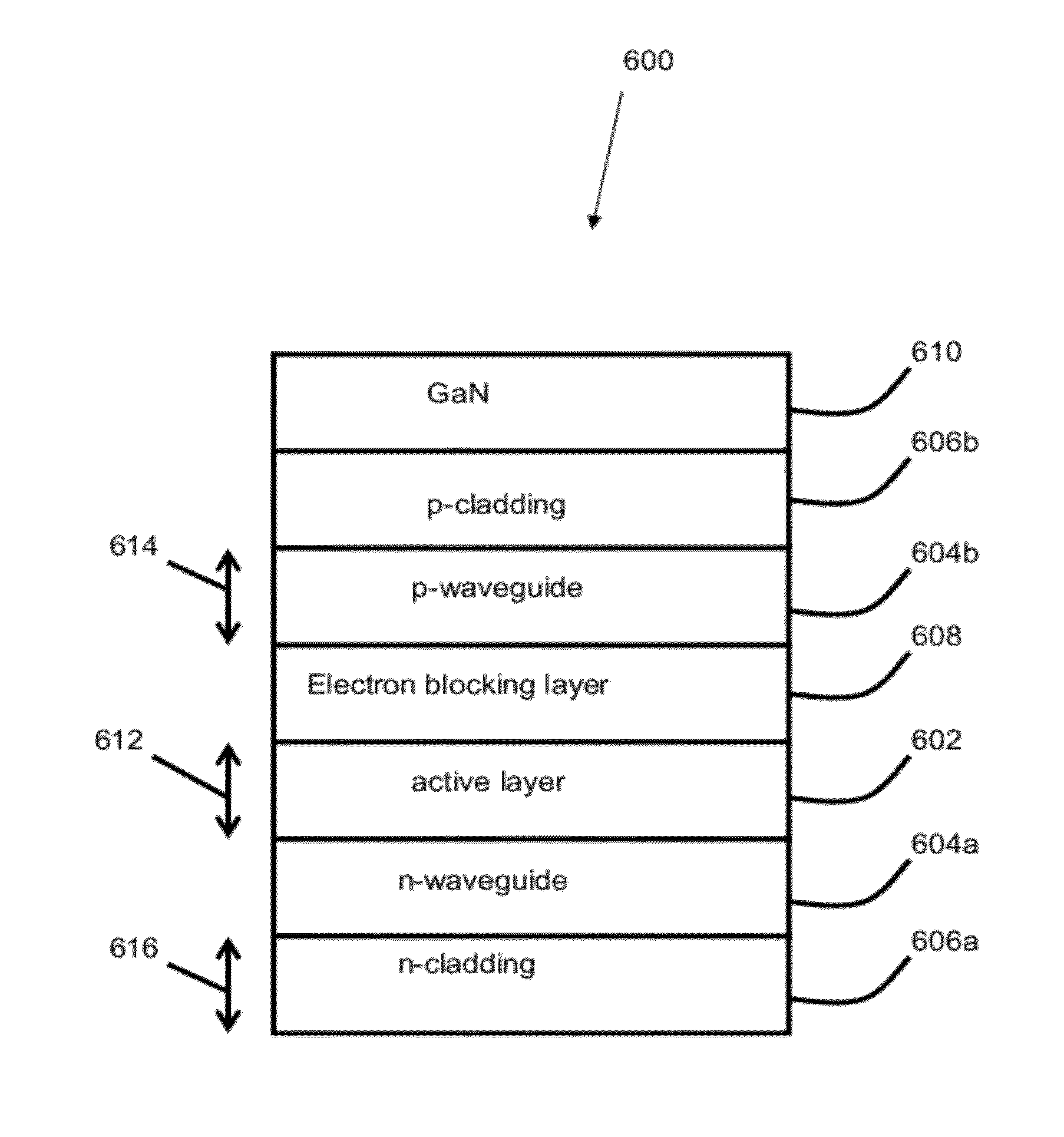
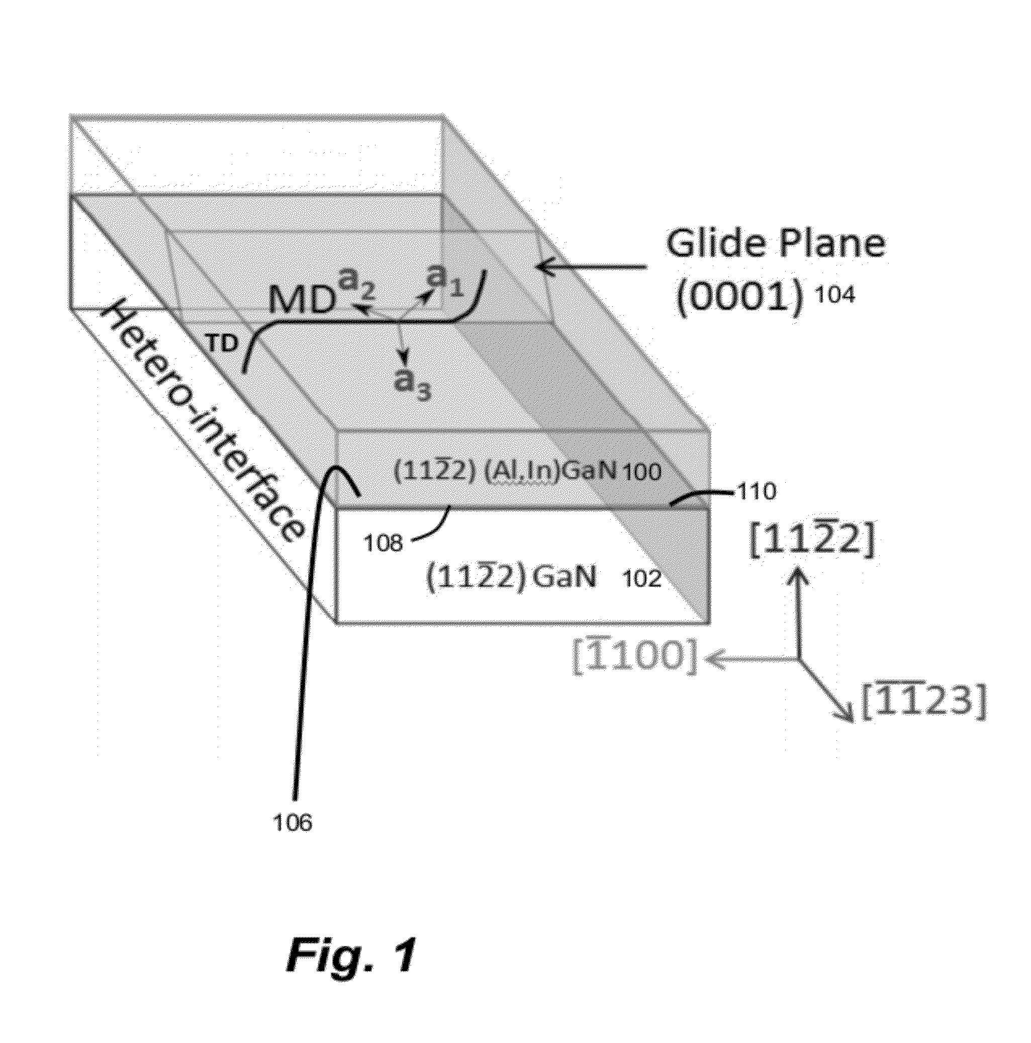
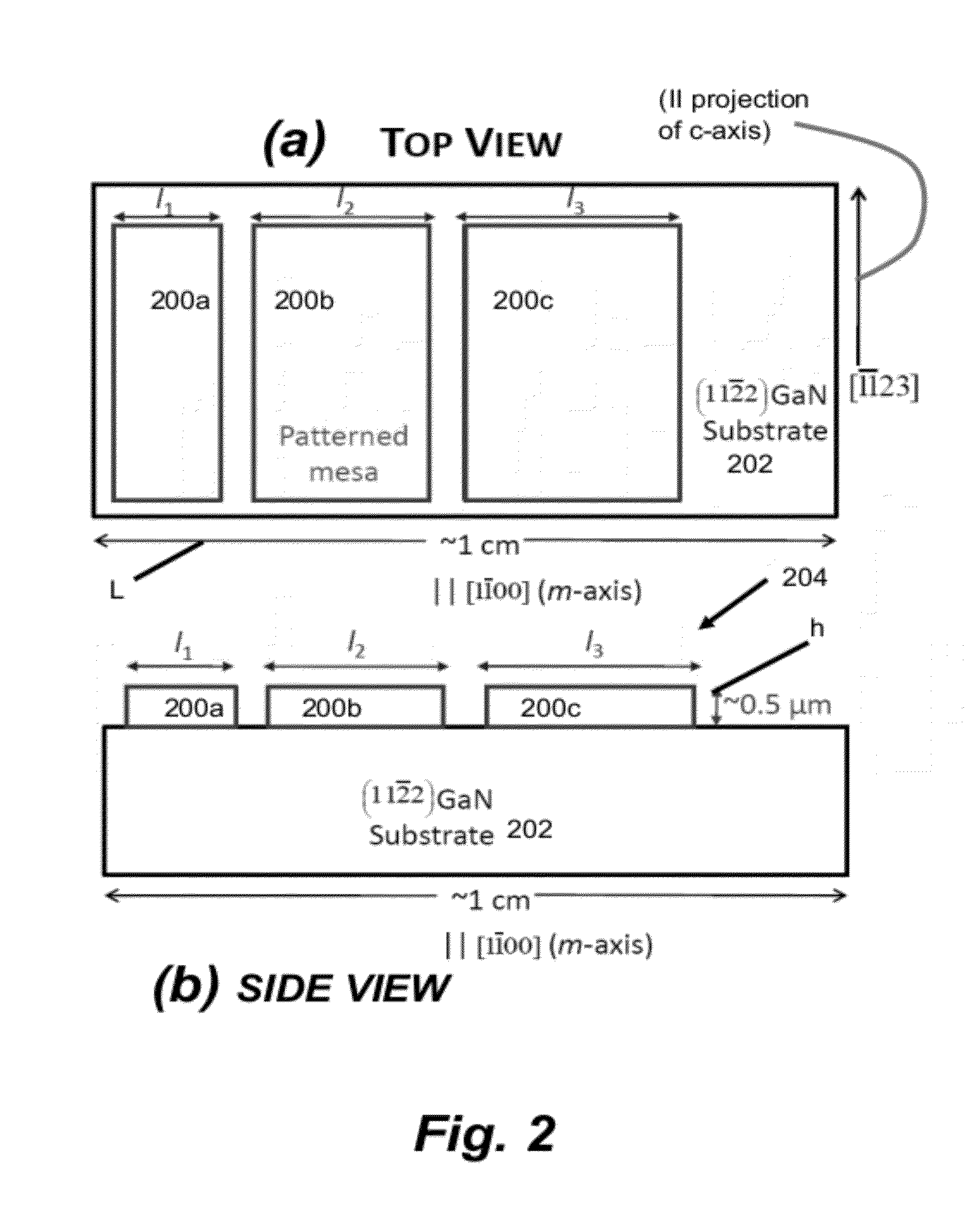
[0032]State of the art commercial III-nitride devices are based on coherent growth of hetero-epitaxial films on a III-nitride substrate. As mentioned above, this limits the thickness / composition of strained III-nitride films and limits the device design space. Using higher composition strained epilayers leads to the formation of MDs at heterointerfaces, which can degrade device performance [1]. The current invention provides a work-around to the MD formation process by limiting the glide length of pre-existing Threading Dislocations (TDs).

[0033]Nomenclature

[0034]GaN and its te...


PUM


Abstract

A method of fabricating a substrate for a semipolar III-nitride device, comprising patterning and forming one or more mesas on a surface of a semipolar III-nitride substrate or epilayer, thereby forming a patterned surface of the semipolar III-nitride substrate or epilayer including each of the mesas with a dimension / along a direction of a threading dislocation glide, wherein the threading dislocation glide results from a III-nitride layer deposited heteroepitaxially and coherently on a non-patterned surface of the substrate or epilayer.

Description

CROSS REFERENCE TO RELATED APPLICATIONS[0001]This application claims the benefit under 35 U.S.C. Section 119(e) of co-pending and commonly-assigned U.S. Provisional Application Ser. No. 61 / 406,876 filed on Oct. 26, 2010, by James S. Speck, Anurag Tyagi, Steven P. DenBaars, and Shuji Nakamura, entitled “LIMITING STRAIN RELAXATION IN III-NITRIDE HETEROSTRUCTURES BY SUBSTRATE AND EPITAXIAL LAYER PATTERNING,” attorney's docket number 30794.387-US-P1 (2010-804), which application is incorporated by reference herein.[0002]This application is related to co-pending and commonly assigned U.S. Utility patent application Ser. No. ______, filed on same date herewith, by James S. Speck, Anurag Tyagi, Alexey Romanov, Shuji Nakamura, and Steven P. DenBaars, entitled “VICINAL SEMIPOLAR III-NITRIDE SUBSTRATES TO COMPENSATE TILT FO RELAXED HETERO-EPITAXIAL LAYERS,” attorney' docket number 30794.386-US-U1 (2010-973), which application claims the benefit under 35 U.S.C. Section 119(e) of co-pending and...

Claims


Application Information

Patent Timeline
Patent Type & Authority Applications(United States)
IPC IPC(8): H01L33/04H01L29/20
CPCB82Y20/00H01L29/045H01L29/2003H01L29/7787H01S2304/12H01L33/16H01S5/3201H01S5/3202H01S5/34333H01L33/0075H01S5/32025H01S5/320275H01L33/30
Inventor SPECK, JAMES S.TYAGI, ANURAGDENBAARS, STEVEN P.NAKAMURA, SHUJI
Owner RGT UNIV OF CALIFORNIA
Why Eureka
Try Eureka