Simplified copper-copper bonding

a technology of copper-copper bonding and copper-copper, applied in the direction of solid-state diffusion coating, coating, chemistry apparatus and processes, etc., can solve the problem that applying pressure may damage the mems sensor

Active Publication Date: 2012-04-26
COMMISSARIAT A LENERGIE ATOMIQUE ET AUX ENERGIES ALTERNATIVES +1
View PDF2 Cites 39 Cited by
  • Summary
  • Abstract
  • Description
  • Claims
  • Application Information

AI Technical Summary

Benefits of technology

[0010]Advantageously, the bonding according to the present invention may be performed at room temperature under atmospheric pressure, in open air, without any adhesive, without any specific pressure and without annealing. By working at room temperature, it is possible to improve the alignment of the wafers to be bonded or of the components borne by the wafers, since the occurrence of a curvature difference between the wafers is avoided.

Problems solved by technology

Applying pressure may damage the MEMS sensors.

Method used


Image

  • Simplified copper-copper bonding
  • Simplified copper-copper bonding
  • Simplified copper-copper bonding

Examples


Embodiment Construction

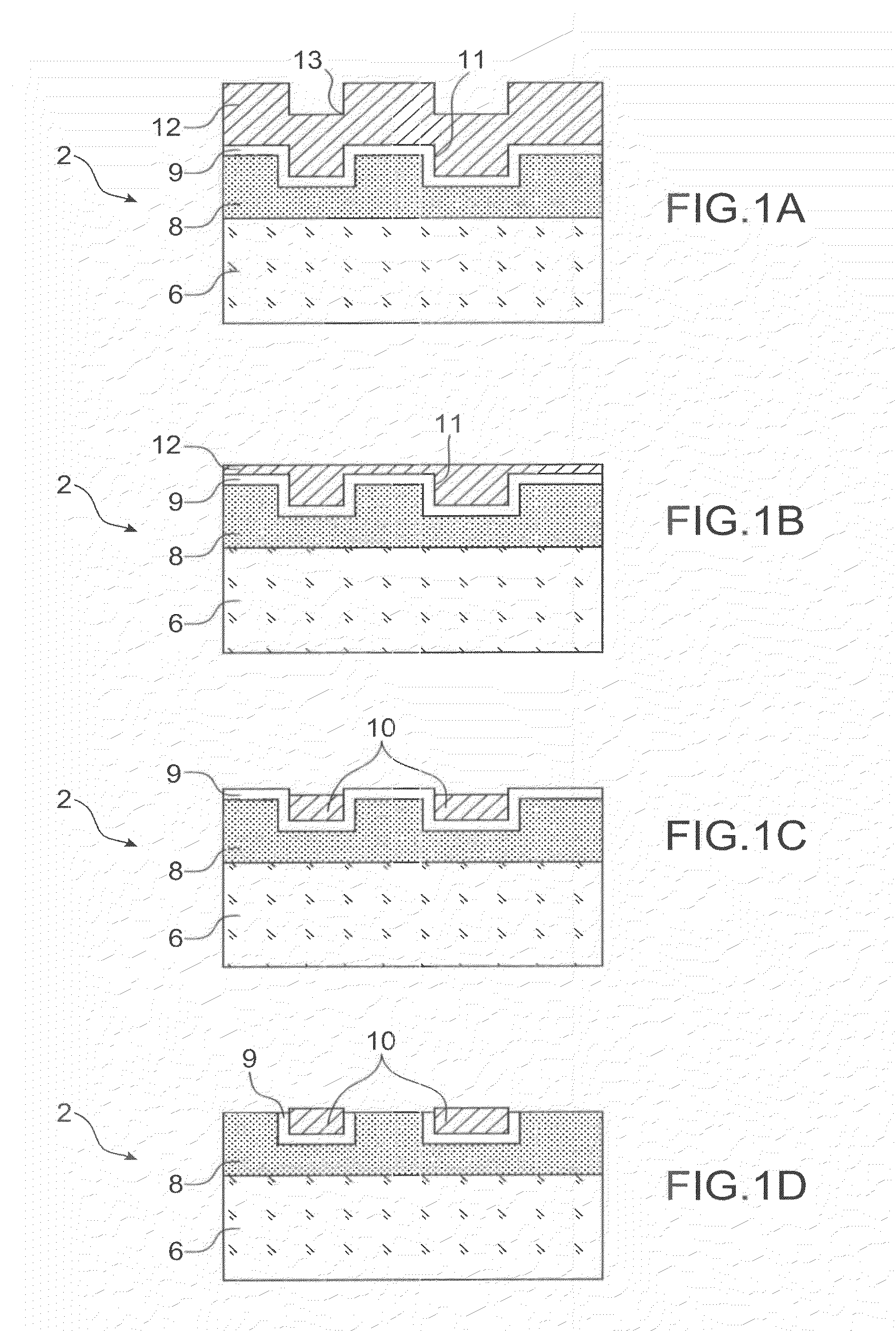
[0048]The method according to the present invention consists of achieving molecular bonding between copper elements.

[0049]Both of these elements may each be a copper plate, a copper layer or connection pads or connection lines, one face of which is flush with a substrate in an insulating material. Or further one of the elements may be a copper plate and the other element a set of pads, one face of which is flush with an insulating substrate.

[0050]Molecular bonding is understood as bonding by molecular adhesion during which two planar surfaces adhere to each other without applying any adhesive.

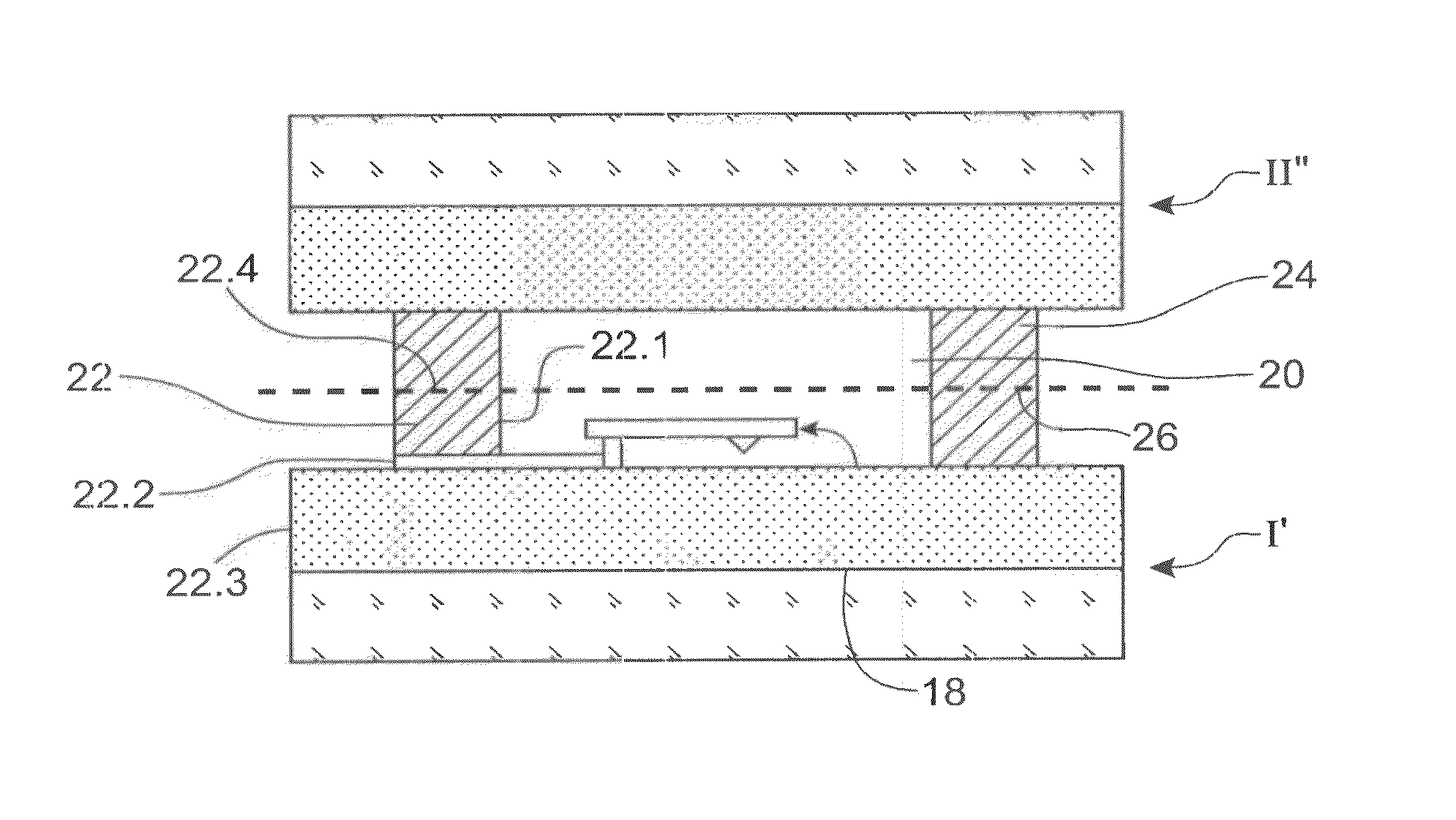
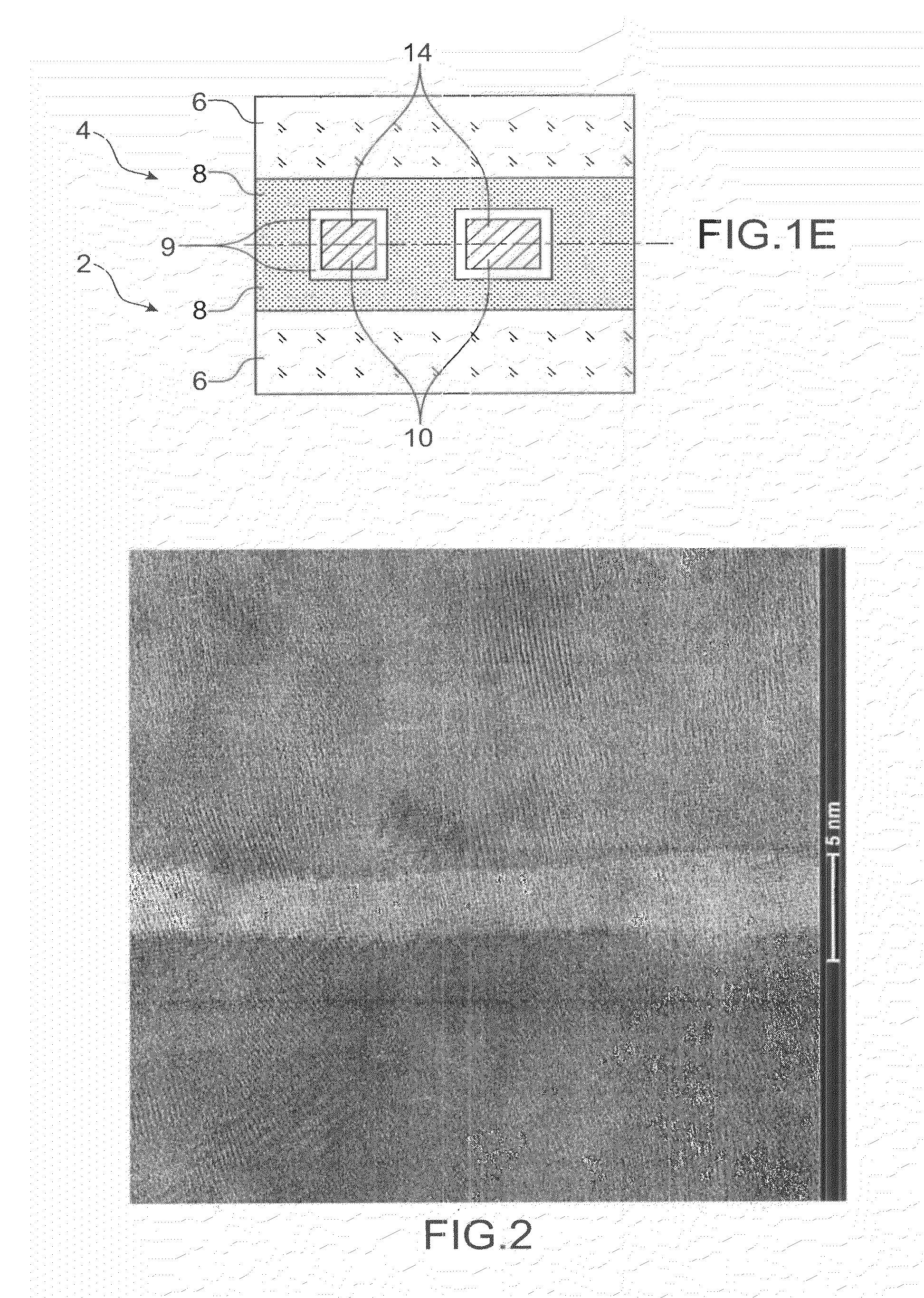
[0051]In FIG. 1A, a schematic illustration of one of the two elements 2, 4 to be bonded may be seen. In the illustrated example, both elements are symmetrical, as this may be seen in FIG. 1E; only one will be described in detail. Element 2 includes a substrate 6, for example in silicon covered with a layer of dielectric material 8, for example in SiO2 and copper pads 10 are made in the dielectr...


PUM

PropertyMeasurementUnit
total thicknessaaaaaaaaaa
roughnessaaaaaaaaaa
roughnessaaaaaaaaaa

Abstract

A method for bonding a first copper element onto a second copper element including forming a crystalline copper layer enriched in oxygen on each of surfaces of each of the first and second elements through which the elements will be in contact, the total thickness of both layers being less than 6 nm, which includes: a) polishing the surfaces so as to obtain a roughness of less than 1 nm RMS, and hydrophilic surfaces, b) cleaning the surfaces to suppress presence of particles due to the polishing and the major portion of corrosion inhibitors, and c) putting both crystalline copper layer enriched in oxygen in contact with each other.

Description

TECHNICAL FIELD AND PRIOR ART[0001]The present invention relates to metal-metal bonding, more particularly to simplified copper-copper bonding, which may notably be used in the manufacturing of microelectronic devices.[0002]Three-dimensional integration in microelectronic devices allows reduction in the size of the devices, reduction of their electric consumption, increase in the transmission rates, the performances, the operating frequency.[0003]A three-dimensional integration notably includes bonding steps with alignment, thinning and vertical interconnection through the stack.[0004]TSV (Through Silicon Via) technology is used, which consists of making connection vias through silicon. However, in order to obtain high interconnection density and to simplify the technology, it is preferable to associate them with metal-metal bonding directly.[0005]Copper is one of the metals particularly used for making connection pads.[0006]There exist different methods for achieving direct copper-...

Claims


Application Information

Patent Timeline
Patent Type & Authority Applications(United States)
IPC IPC(8): H01L21/00C23C8/04C23C8/80
CPCB81C1/00269B81C1/00301H01L2924/1461B81C2203/0109B81C2203/019B81C2203/038H01L24/03H01L24/05H01L24/08H01L24/80H01L2224/80895H01L2224/08148H01L2224/80357H01L2224/80896H01L2924/00H01L2224/05547H01L2224/80986B32B15/01B81C1/00C23C10/28H01L21/02
Inventor DI CIOCCIO, LEAGUEGUEN, PIERRICRIVOIRE, MAURICE
Owner COMMISSARIAT A LENERGIE ATOMIQUE ET AUX ENERGIES ALTERNATIVES
Why Eureka
Try Eureka