Solid-state image pickup device

a solid-state image and pickup device technology, applied in the field of solid-state image pickup devices, can solve the problems of increasing the integral value of random noise, limited amplifier bandwidth, increasing signal bandwidth, etc., and achieve the effect of reducing random noise and improving the signal-to-noise ratio

Inactive Publication Date: 2012-05-03
CANON KK
View PDF4 Cites 14 Cited by
  • Summary
  • Abstract
  • Description
  • Claims
  • Application Information

AI Technical Summary

Benefits of technology

[0006]The present invention provides a solid-state image pickup device capable of reducing random noise generated from an amplifying circuit and improving a signal-to-noise (S / N) ratio.

Problems solved by technology

Such an increase in signal bandwidth leads to an increase in the integral value of random noise, which is proportional to the signal bandwidth of the amplifier.
As a result of clamping the reference potential of the amplifier by connecting a capacitor to the output end of the amplifier, the bandwidth of the amplifier is limited.
However, in the case of changing the amplification factors of amplifiers in accordance with an image capturing condition, the driving method according to Japanese Patent Laid-Open No. 2008-78894 does not always sufficiently reduce random noise generated from the amplifiers.
For this reason, the frequency band of the amplifier becomes wider as the amplification factor decreases with a small feedback capacitance, and random noise increases in proportion to the frequency bandwidth.
In other words, random noise generated from the amplifier is not always sufficiently reduced depending on an amplification factor that is set.

Method used


Image

  • Solid-state image pickup device
  • Solid-state image pickup device
  • Solid-state image pickup device

Examples


first embodiment

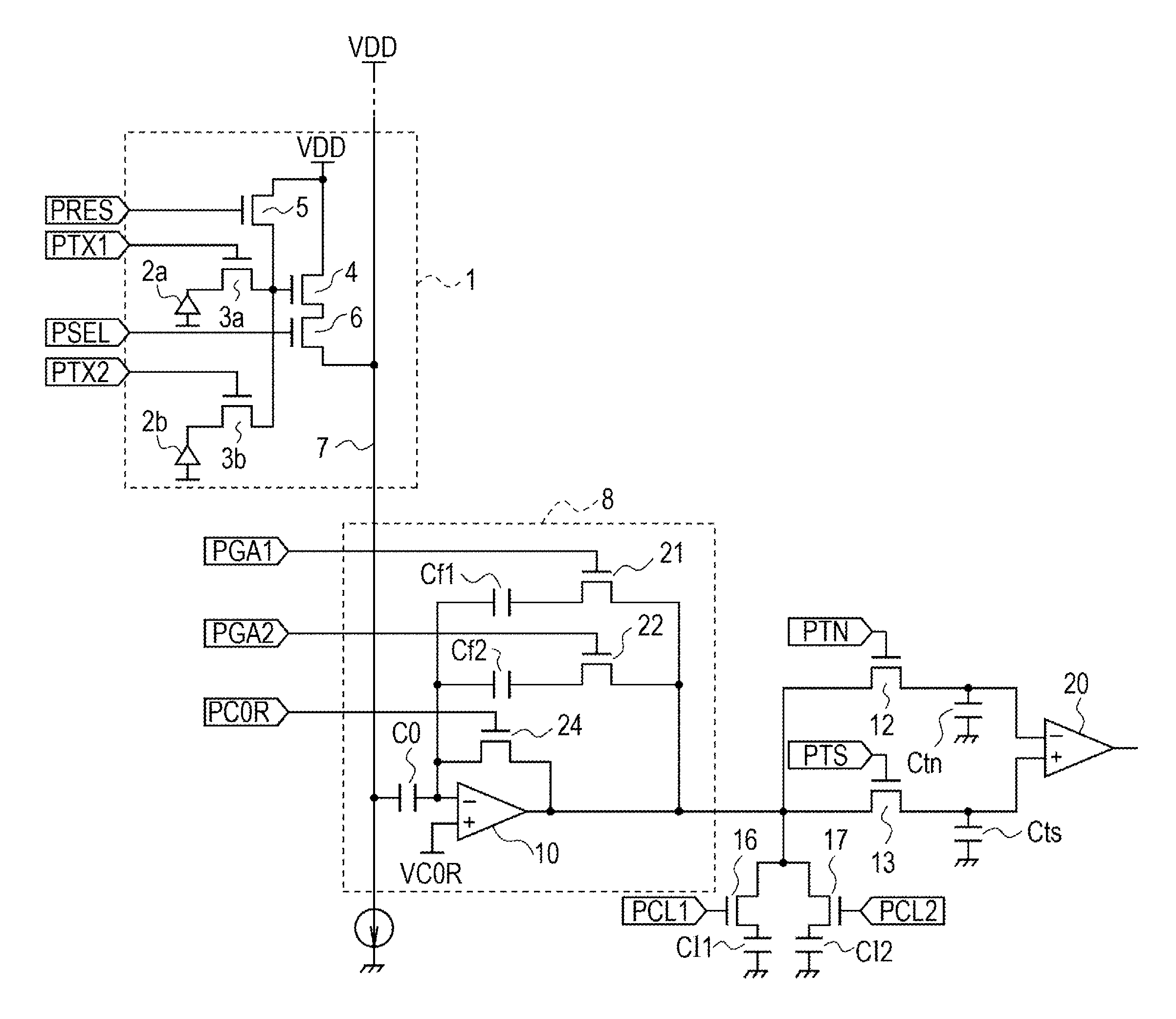
[0021]FIG. 1 is an equivalent circuit diagram of a pixel section and a readout circuit for one column of a solid-state image pickup device according to a first embodiment of the present invention. As for the pixel section, pixels in two rows and one column among a plurality of pixels that are two-dimensionally arranged are illustrated. The pixel section 1 includes photoelectric conversion elements 2a and 2b, transfer transistors 3a and 3b, a source follower transistor 4, a reset transistor 5, and a row-selection transistor 6. Metal-oxide semiconductor (MOS) transistors may be used as these transistors. Hereinafter, the transfer transistors 3a and 3b are referred to as transfer MOSs 3a and 3b, the source follower transistor 4 is referred to as an SFMOS 4, the reset transistor 5 is referred to as a reset MOS 5, and the row-selection transistor 6 is referred to as a row-selection MOS 6. The photoelectric conversion elements 2a and 2b are photodiodes, for example, which are provided in ...

second embodiment

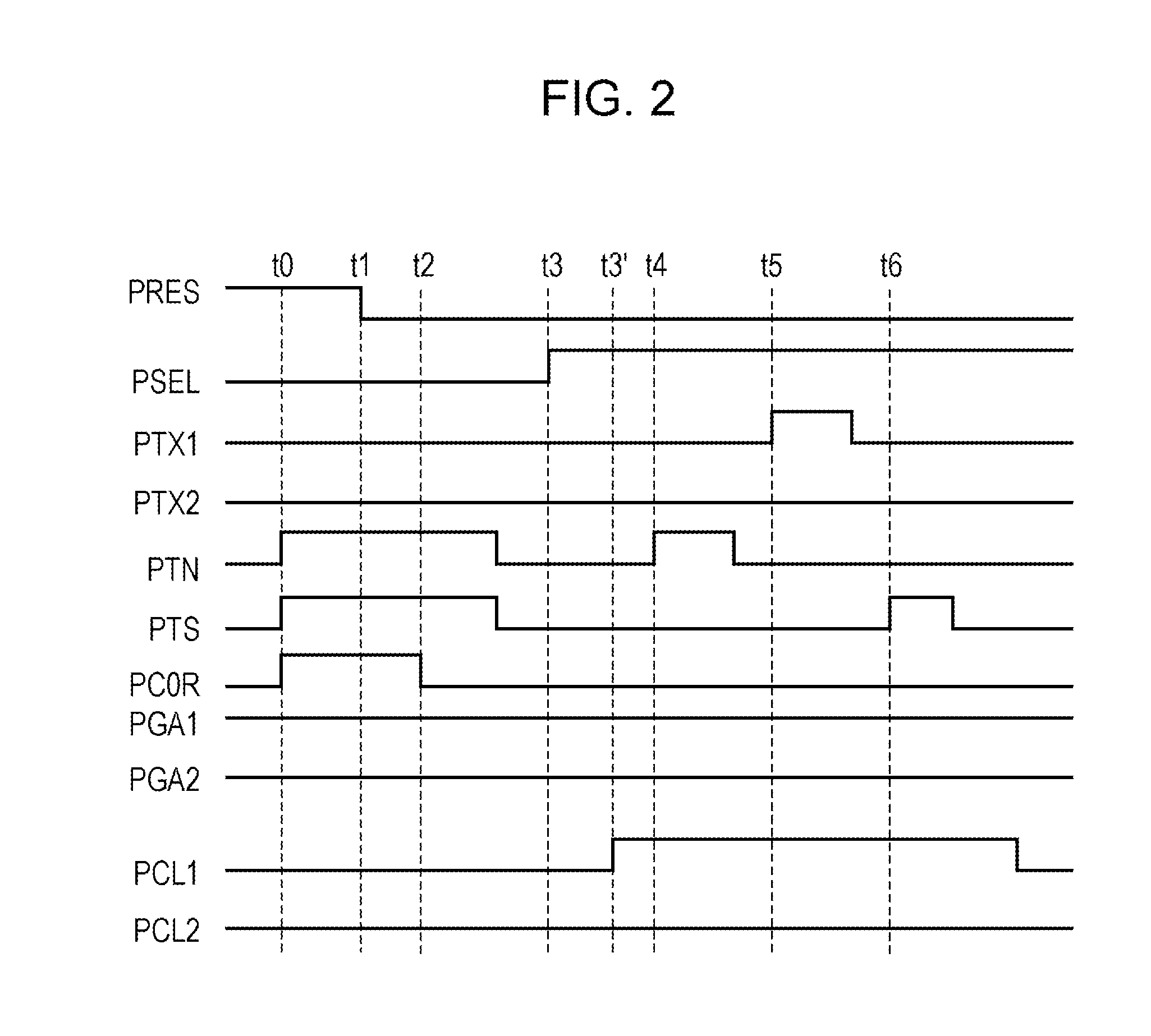
[0045]Hereinafter, a description will be given of a solid-state image pickup device according to a second embodiment of the present invention and a method for driving the solid-state image pickup device. The circuit diagram of the solid-state image pickup device according to the second embodiment is the same as that illustrated in FIG. 1 according to the first embodiment. FIG. 5 is a timing chart illustrating an exemplary operation of the solid-state image pickup device (FIG. 1) according to the second embodiment. The timing chart in FIG. 5 is different from the timing chart in FIG. 2 regarding the signals PCL1 and PCL2. Hereinafter, the points different from the timing chart in FIG. 2 will be described with reference to FIG. 5. The amplification factor of the amplifying circuit unit 8 is the same as that in FIG. 2, that is, C0 / (Cf1+Cf2). At time to, the levels of the signals PCL1 and PCL2 are changed to be high. Accordingly, the control switches 16 and 17 are turned on, and the out...

third embodiment

[0051]A solid-state image pickup device according to a third embodiment of the present invention is realized by combining the first and second embodiments. The circuit diagram of the solid-state image pickup device according to the third embodiment is the same as that illustrated in FIG. 1. FIG. 7 is a timing chart illustrating an exemplary operation of the solid-state image pickup device according to the third embodiment. The timing chart in FIG. 7 is different from the timing chart in FIG. 5 regarding the signal PCL1. Hereinafter, the points different from the timing chart in FIG. 5 will be described with reference to FIG. 7. As in FIG. 2, at time t3′ after time t3, the level of the signal PCL1 is changed to be high again. Accordingly, the control switch 16 is turned on, and the output node of the amplifying circuit unit 8 is connected to the load capacitor Cl1. Then, after time t6, the level of the signal PCL1 is changed to be low. Accordingly, the control switch 16 is turned off...


PUM


Abstract

A solid-state image pickup device includes a pixel including a photoelectric conversion element that converts light into an electric signal, a feedback amplifying circuit that amplifies a signal of the pixel using an amplification factor that is based on a variable feedback capacitor, a storage capacitor connected to an output node of the amplifying circuit via a first switch, and a load element connected to the output node of the amplifying circuit via a second switch. The second switch is in an on state during any one of or both of a period in which the feedback capacitor is reset and a period in which the first switch is in an on state.

Description

BACKGROUND OF THE INVENTION[0001]1. Field of the Invention[0002]The present invention relates to solid-state image pickup devices used for digital still cameras, digital video cameras, or the like.[0003]2. Description of the Related Art[0004]In typical solid-state image pickup devices, electric signals that are generated through photoelectric conversion performed in a plurality of pixels arranged in a two-dimensional matrix are transmitted to a signal processing circuit in the subsequent stage via amplifiers provided in the respective columns. In recent years, there has been a demand for solid-state image pickup devices to have more pixels and to operate at higher speed, so that the bandwidth set in each amplifier has tended to be wide. Such an increase in signal bandwidth leads to an increase in the integral value of random noise, which is proportional to the signal bandwidth of the amplifier. Japanese Patent Laid-Open No. 2008-78894 describes a configuration in which a capacitor i...

Claims


Application Information

Patent Timeline
Patent Type & Authority Applications(United States)
IPC IPC(8): H04N5/335
CPCH03G5/28H04N5/243H04N5/347H04N5/357H04N5/363H04N5/37457H04N5/378H04N23/76H04N25/46H04N25/65H04N25/60H04N25/778H04N25/75
Inventor IIDA, SATOKO
Owner CANON KK
Why Eureka
Try Eureka