

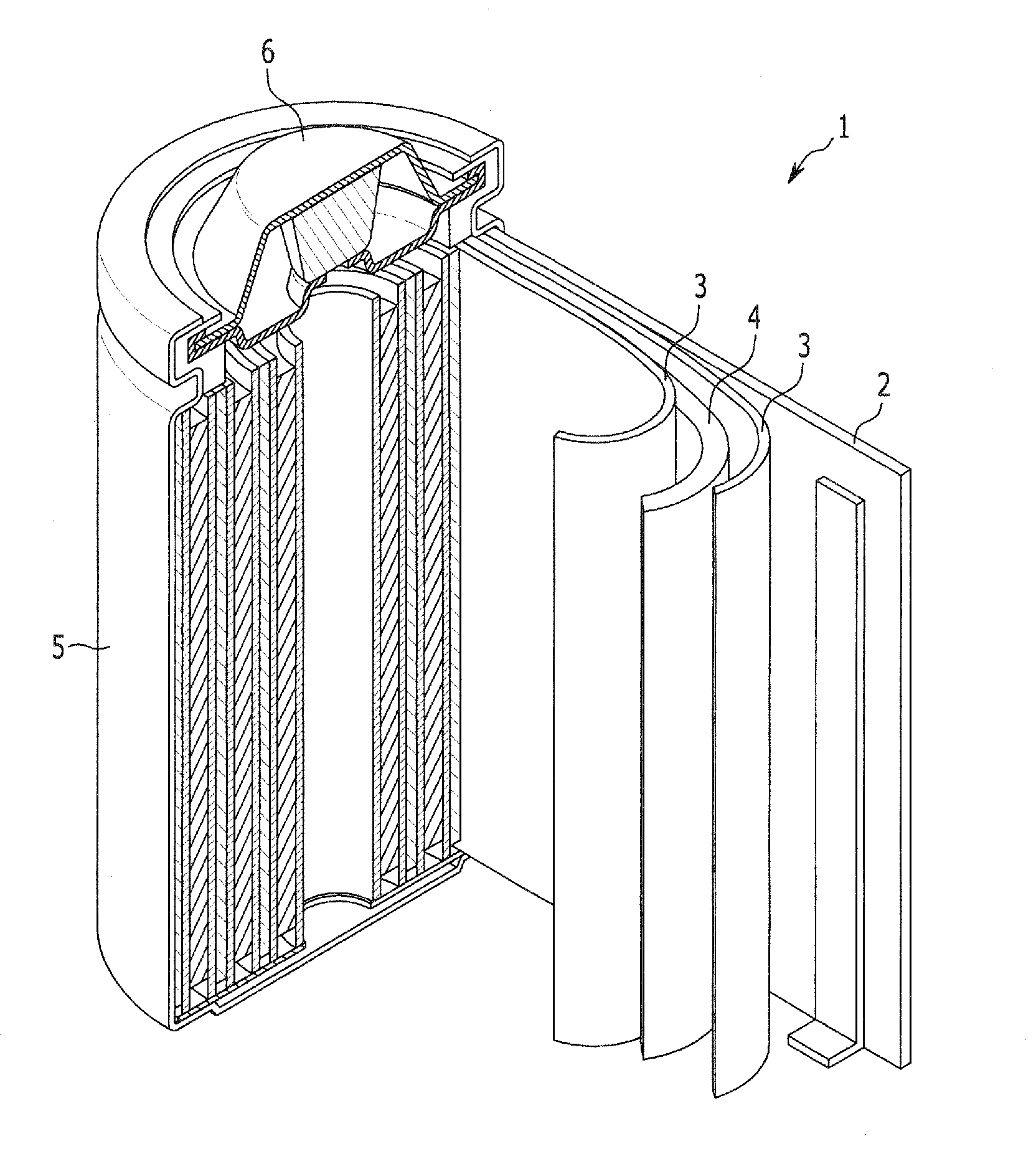
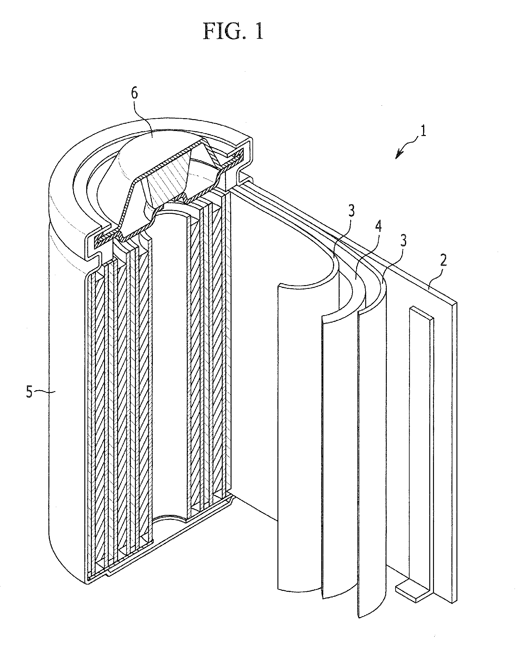
Negative active material for rechargeable lithium battery and rechargeable lithium battery
a technology of active materials and rechargeable lithium batteries, which is applied in the manufacture of electrodes, carbides, cell components, etc., can solve the problems of generating gas, deterioration of capacity, and deterioration of energy density, and achieve excellent initial charge and discharge efficiency and cycle-life characteristics, high energy density and excellent effect of energy density
- Summary
- Abstract
- Description
- Claims
- Application Information
AI Technical Summary
Benefits of technology
Problems solved by technology
Method used
Image

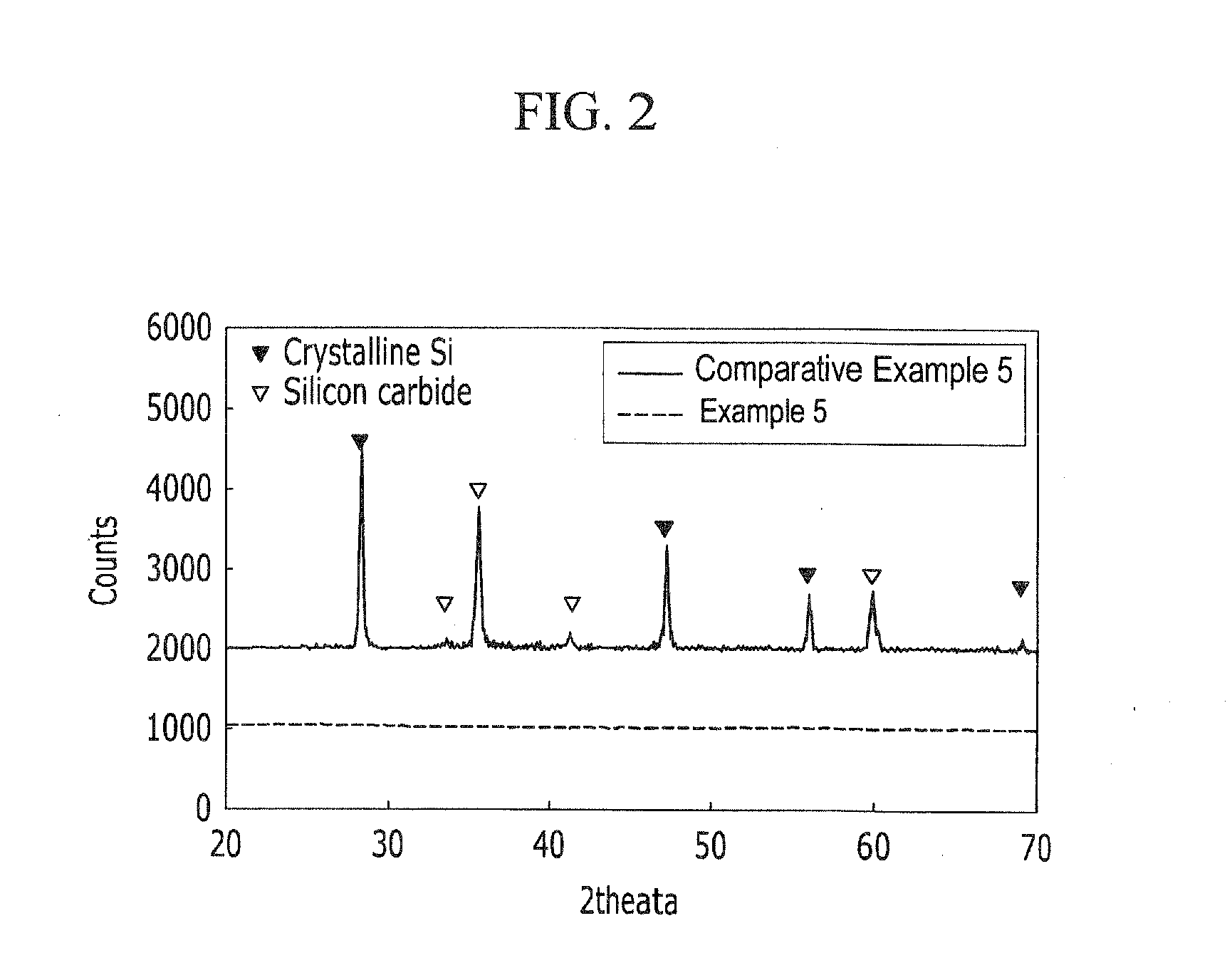
Examples
example 1
[0087]2 μm-thick amorphous SiCx (x=0.65) layer was formed on a 20 μm-thick Cu foil using a two-sources sputtering apparatus, a Si target, and a C target through a sputtering process. Outputs for the Si target and the C target were respectively set to be 400 W and 200 W.
[0088]The concentration ratio, A (C / Si mole ratio), was 0.65 at the center of the SiCx (x=0.65) layer (near close by the Cu foil), and the concentration ratio, B (C / Si mole ratio) was 0.65 at a surface area, which was identified through XPS. The surface area was referred to be 20% of a depth in a direction from the surface to the Cu foil based on 100% thickness of the amorphous SiCx (x=0.65) layer.
[0089]The fabricated product including a SiCx (x=0.65) layer (negative active material layer) on a Cu foil was used as a negative electrode.
example 2
[0090]2 μm-thick amorphous SiCx (x=0.65) layer was formed according to the same method as Example 1, except that using a two-source sputtering apparatus, a Si target, and a C target, a sputtering process was performed on a 20 μm-thick Cu foil while keeping an output for a Si target to be 400 W and gradually changing an output for a C target from initial output 600 W to 100 W. The concentration ratio A(C / Si mole ratio) was 0.95 at the center of the SiCx (x=0.65) layer (close by the Cu foil), and the concentration ratio B (C / Si mole ratio) was 0.2 at a surface area. The surface area was referred to be 20% of a depth in a direction from the surface to the Cu foil based on 100% thickness of the amorphous SiCx (x=0.65) layer.
example 3
[0091]2 μm-thick amorphous SiCx (x=0.05) layer was formed according to the same method as Example 1, except that using a two-source sputtering apparatus, a Si target, and a C target, a sputtering process was performed on a 20 μm-thick Cu foil, while keeping an output for a Si target to be 600 W and gradually changing an output for a C target from initial output 100 W to 30 W. The concentration ratio A (C / Si mole ratio) was 0.1 at the center of the SiCx (x=0.05) layer (close by the Cu foil), and the concentration ratio B (C / Si mole ratio) was 0.03 at a surface area. The surface area was referred to be 20% The surface area was referred to be 20% of a depth in a direction from the surface to the Cu foil based on 100% thickness of the amorphous SiCx (x=0.05) layer.
PUM
 Abstract
Description
Claims
Application Information