

Fall detectors and a method of detecting falls
- Summary
- Abstract
- Description
- Claims
- Application Information
AI Technical Summary
Benefits of technology
Problems solved by technology
Method used
Image

Examples
first embodiment
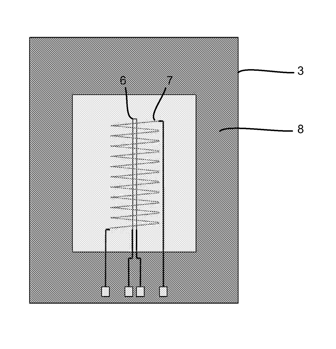
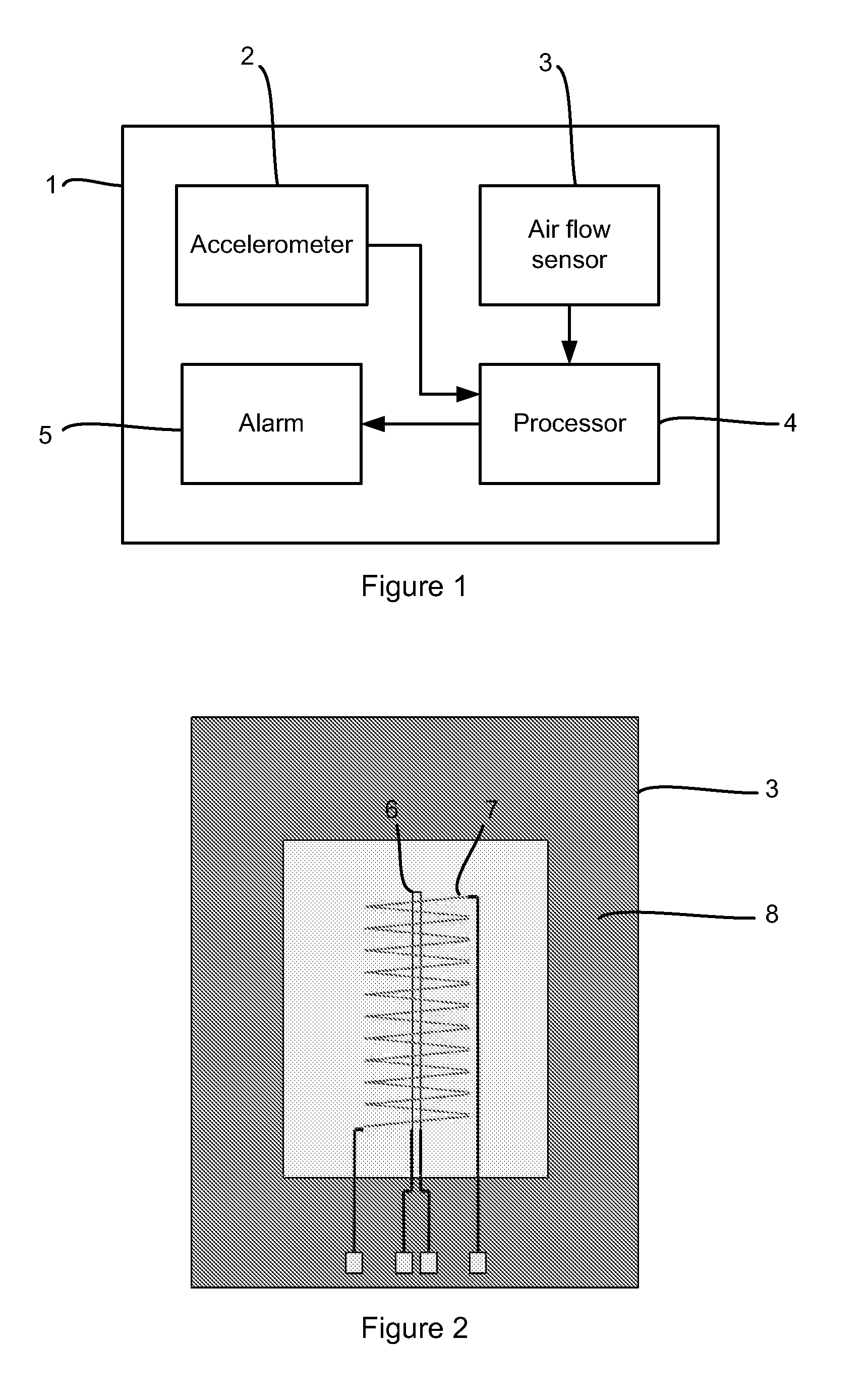
[0051]In some embodiments of the thermal flow sensor, there is a metal layer on the front side of the integrated circuit, for electrical connection between the sensing element and the bond pad, and the bond pad comprises the back side of the metal layer. This enables the bond pad to be relatively close to the sensing element to keep the structure simple and compact. An example is shown in the thermal flow sensor described below.
[0052]In some embodiments of the thermal flow sensor, the integrated circuit comprises a substrate and the substrate is patterned to provide an aperture to expose the bond pad to enable contact to the bond pad through the aperture. This can help protect the contact and provide a compact structure.
second embodiment
[0053]In some embodiments of the thermal flow sensor the integrated circuit comprises a substrate and the substrate is patterned to form one or more pillars, and the bond pad is located on a back side of the substrate on one of the pillars. The pillars can provide support for the bond pad, and maintain isolation from other circuitry. An example is shown in the thermal flow sensor described below.
[0054]In some embodiments of the thermal flow sensor the integrated circuit comprises a heating element on a front side of the integrated circuit to face the fluid channel. This enables a more integrated solution, though in alternative embodiments of the thermal flow sensor, the heating can be provided by a heater external to the integrated circuit. The external heater should be provided so that the fluid is heated sufficiently closely to the temperature sensor.
third embodiment
[0055]In some embodiments of the thermal flow sensor the integrated circuit comprises a silicon on insulator integrated circuit. This helps enable other circuit elements to be integrated. the thermal flow sensor described below discloses this arrangement.
PUM
| Property | Measurement | Unit |
|---|---|---|
| Temperature | aaaaa | aaaaa |
| Electrical conductor | aaaaa | aaaaa |
| Altitude | aaaaa | aaaaa |
Abstract
Description
Claims
Application Information