Adhesive film for semiconductor device, and semiconductor device
What is AI technical title?
AI technical title is built by Patsnap AI team. It summarizes the technical point description of the patent document.
a technology for adhesive films and semiconductors, applied in the directions of layered products, transportation and packaging, chemistry apparatuses and processes, etc., can solve the problem that the sheet does not function well as an electromagnetic wave shielding material
Inactive Publication Date: 2012-05-24
NITTO DENKO CORP
View PDF3 Cites 26 Cited by
Summary
Abstract
Description
Claims
Application Information
AI Technical Summary
This helps you quickly interpret patents by identifying the three key elements:
Problems solved by technology
Method used
Benefits of technology
Benefits of technology
[0013]According to the above-described configuration, the attenuation of the electromagnetic wave that penetrates the adhesive film for a semiconductor device is 3 dB or more in at least a portion of the relatively high frequency range of 50 MHz to 20 GHz, and the electromagnetic wave can be efficiently shielded. Therefore, the influence of an electromagnetic wave emitted from one semiconductor element on other semiconductor chips, the substrate, adjacent devices, and the package can be decreased. Because a relatively high frequency band (for example, a 2 GHz band or a 5.8 GHz band) is used in portable terminals such as a portable telephones and electronic toll collection (ETC) systems, noise from a chip that is generated during communication also is in the high frequency band.
[0014]According to the above-described configuration, an electromagnetic wave of such high frequency band can be efficiently shielded in particular.
Problems solved by technology
However, there is no substantial shielding effect for an electromagnetic wave having a frequency of 100 kHz or more with the thickness described in that patent, and the sheet does not function well as an electromagnetic wave shielding material.
Method used
Image
Click on the blue label to locate the original text in one second.
Reading with bidirectional positioning of images and text.
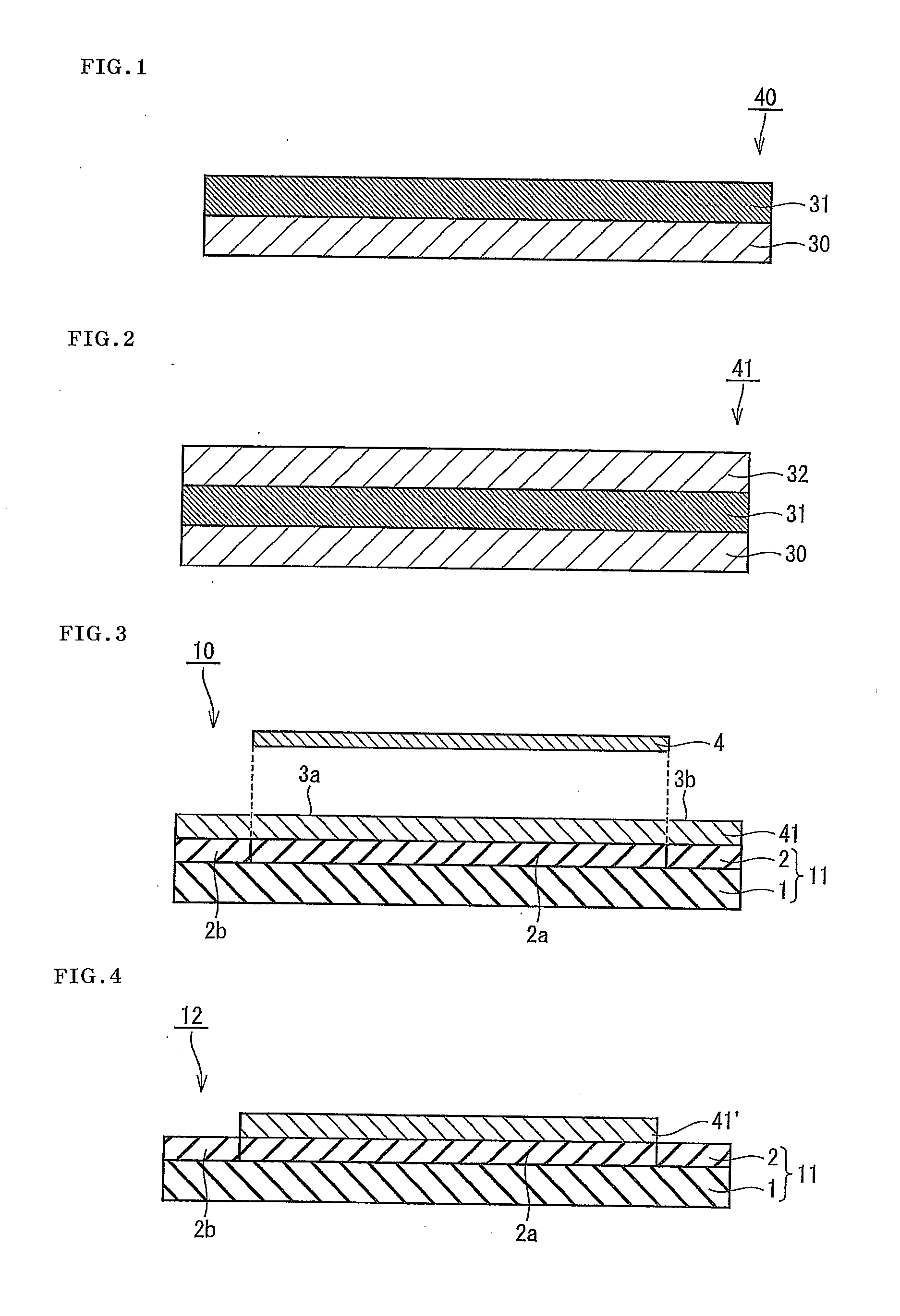
[0157]Adhesive composition solutions having a concentration of 23.6% by weight were obtained by dissolving the following (a) to (f) in methylethylketone.
[0158](a) 100 parts of an acrylic ester polymer having ethyl acrylate-methyl methacrylate as a main component (Paracron W-197CM manufactured by Negami Chemical Industries Co., Ltd.)
[0159](b) 242 parts of an epoxy resin 1 (Epicoat 1004 manufactured by Japan Epoxy Resin Co., Ltd.)
[0160](c) 220 parts of an epoxy resin 2 (Epicoat 827 manufactured by Japan Epoxy Resin Co., Ltd.)
[0161](d) 489 parts of a phenol resin (Milex XLC-4L manufactured by Mitsui Chemicals, Inc.)
[0162](e) 660 parts of spherical silica (SO-25R manufactured by Admatechs Co., Ltd.)
[0163](f) 3 parts of a thermosetting catalyst (C11-Z manufactured by Shikoku Chemicals Corporation)
[0164]An adhesive layer A having a thickness of 60 μm was produced by applying this adhesive composition solution onto a release-treated film (a release liner) made...
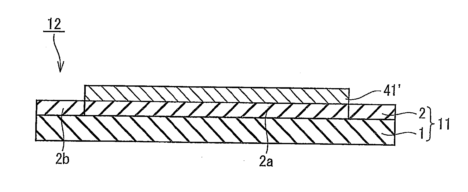
[0172]An adhesive film for a semiconductor device having a thickness of 108 μm was produced by pasting a SUS304 (stainless steel) foil having a thickness of 38 μm between the adhesive layer A and the adhesive layer B under conditions of a temperature of 80° C., a pasting pressure of 0.3 MPa, and a pasting speed of 10 mm / sec. The SUS304 foil has a function as an electromagnetic wave shielding layer.
example 3
Production of Adhesive Film for Semiconductor Device
[0173]An aluminum layer having a thickness of 500 nm was formed on the adhesive layer A by a sputtering method using a sputteringmachine (SH-550 manufactured by ULVAC, Inc.). The sputtering conditions were as follows.
[0175]Then, an adhesive film for a semiconductor device having a thickness of 70.5 μm was produced by pasting the adhesive layer B onto an aluminum layer under conditions of a temperature of 80° C., a pasting pressure of 0.3 MPa, and a pasting speed of 10 mm / sec. The aluminum layer has a function as an electromagnetic wave shielding layer.
PUM
Property
Measurement
Unit
Temperature
aaaaa
aaaaa
Pressure
aaaaa
aaaaa
Frequency
aaaaa
aaaaa
Abstract
An object of the present invention is to decrease the influence of an electromagnetic wave emitted from one semiconductorchip on other semiconductor chips in the same package, amounted substrate, adjacent devices, and the package. The present invention provides an adhesive film for a semiconductor device having an adhesive layer and an electromagnetic wave shielding layer, in which the attenuation of the electromagnetic wave that penetrates the adhesive film for a semiconductor device is 3 dB or more in at least a portion of the frequency range of 50 MHz to 20 GHz.
Description
BACKGROUND OF THE INVENTION[0001]1. Field of the Invention[0002]The present invention relates to an adhesive film for a semiconductor device used in manufacturing a semiconductor device. The present invention also relates to a semiconductor device having the adhesive film for a semiconductor device.[0003]2. Description of the Related Art[0004]In recent years, the wiring width of power supply lines that are arranged across the whole area of the main surface of a semiconductor chip (a semiconductor element) and the space between signal lines have become narrower in order to correspond to demands for microfabrication and high function of semiconductor devices. Because of this, an increase of impedance and an interference between signals in signal lines of different nodes occur, which have become an impediment to sufficient performance in operating speed, the degree of operating voltage margin, and anti-electrostatic breakdown strength of the semiconductor chip.[0005]Conventionally, a p...
Claims
Application Information
Patent Timeline
Application Date:The date an application was filed.
Publication Date:The date a patent or application was officially published.
First Publication Date:The earliest publication date of a patent with the same application number.
Issue Date:Publication date of the patent grant document.
PCT Entry Date:The Entry date of PCT National Phase.
Estimated Expiry Date:The statutory expiry date of a patent right according to the Patent Law, and it is the longest term of protection that the patent right can achieve without the termination of the patent right due to other reasons(Term extension factor has been taken into account ).
Invalid Date:Actual expiry date is based on effective date or publication date of legal transaction data of invalid patent.

