Method for forming isolation trenches

a technology of isolation trenches and trenches, which is applied in the direction of solid-state devices, electric devices, basic electric elements, etc., can solve the problems of affecting the device degrading neighboring circuit performance, and reducing the performance of neighboring devices, so as to reduce the negative impact of neighboring devices of 3d-tsv

Active Publication Date: 2012-06-07
INTERUNIVERSITAIR MICRO ELECTRONICS CENT (IMEC VZW)
View PDF9 Cites 51 Cited by
  • Summary
  • Abstract
  • Description
  • Claims
  • Application Information

AI Technical Summary

Benefits of technology

[0010]Through Substrate Via (TSV) interconnects, such as Through Silicon Via interconnects for use in 3D stacked semiconductor devices, are prov

Problems solved by technology

The negative impact may be mechanical stress created in the substrate around said 3D-TSV structure thereby causing mobility variations in the surrounding substrate and hence resulting in performance degradation of neighboring devices.
The negative impact may be caused by inducing a relatively large electrical capacitance that degrades nei

Method used


Image

  • Method for forming isolation trenches
  • Method for forming isolation trenches
  • Method for forming isolation trenches

Examples


Embodiment Construction

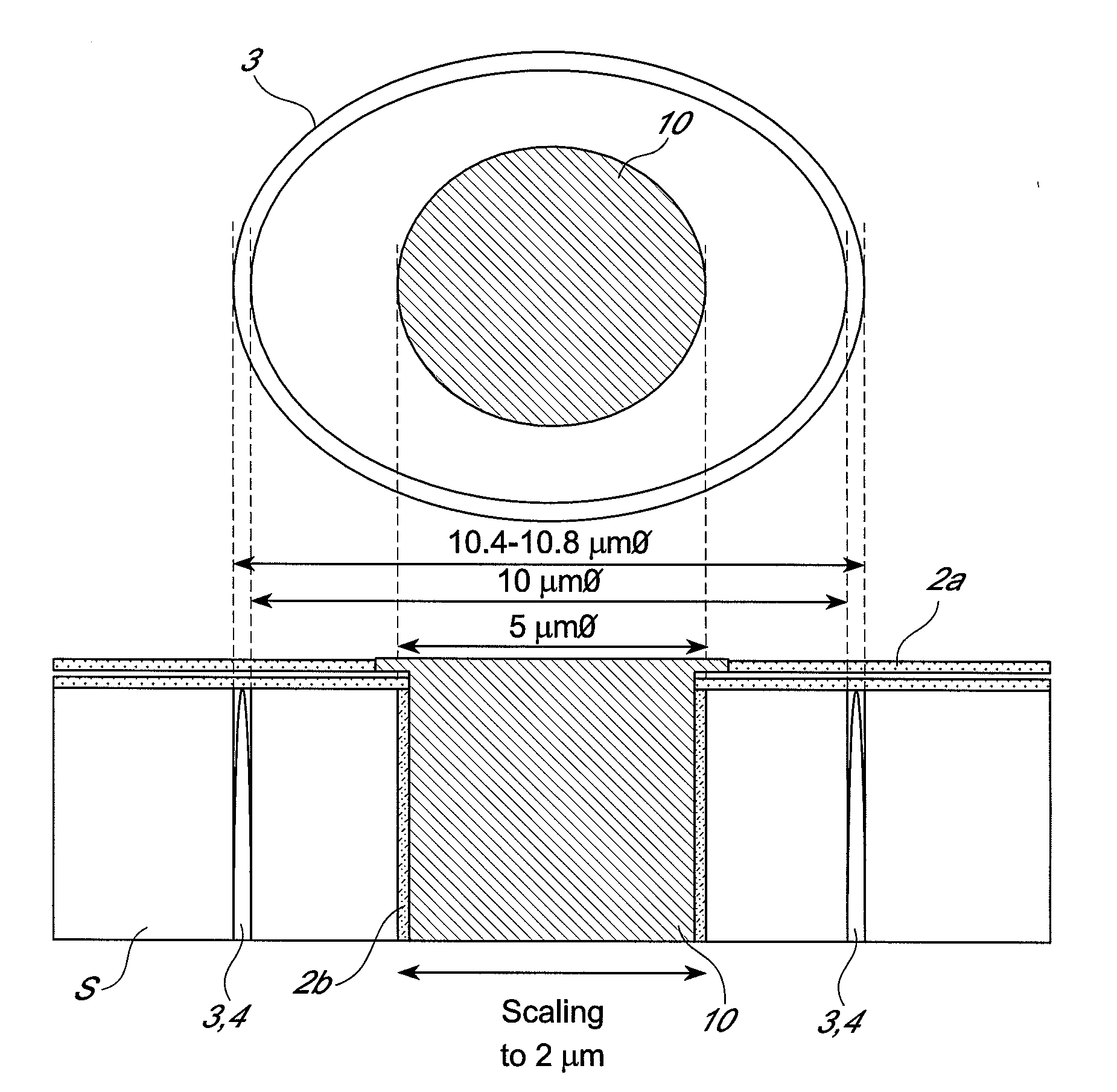
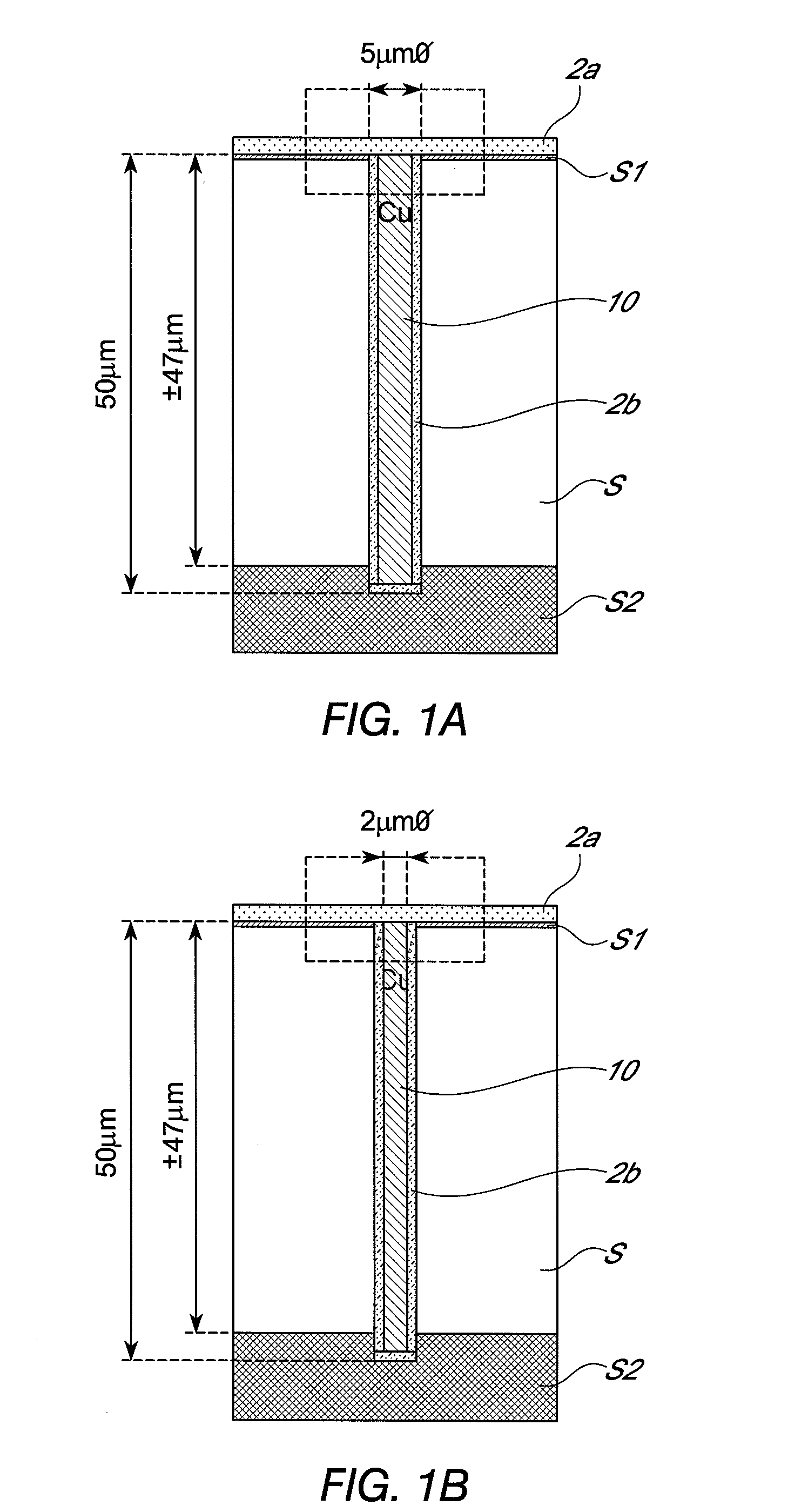
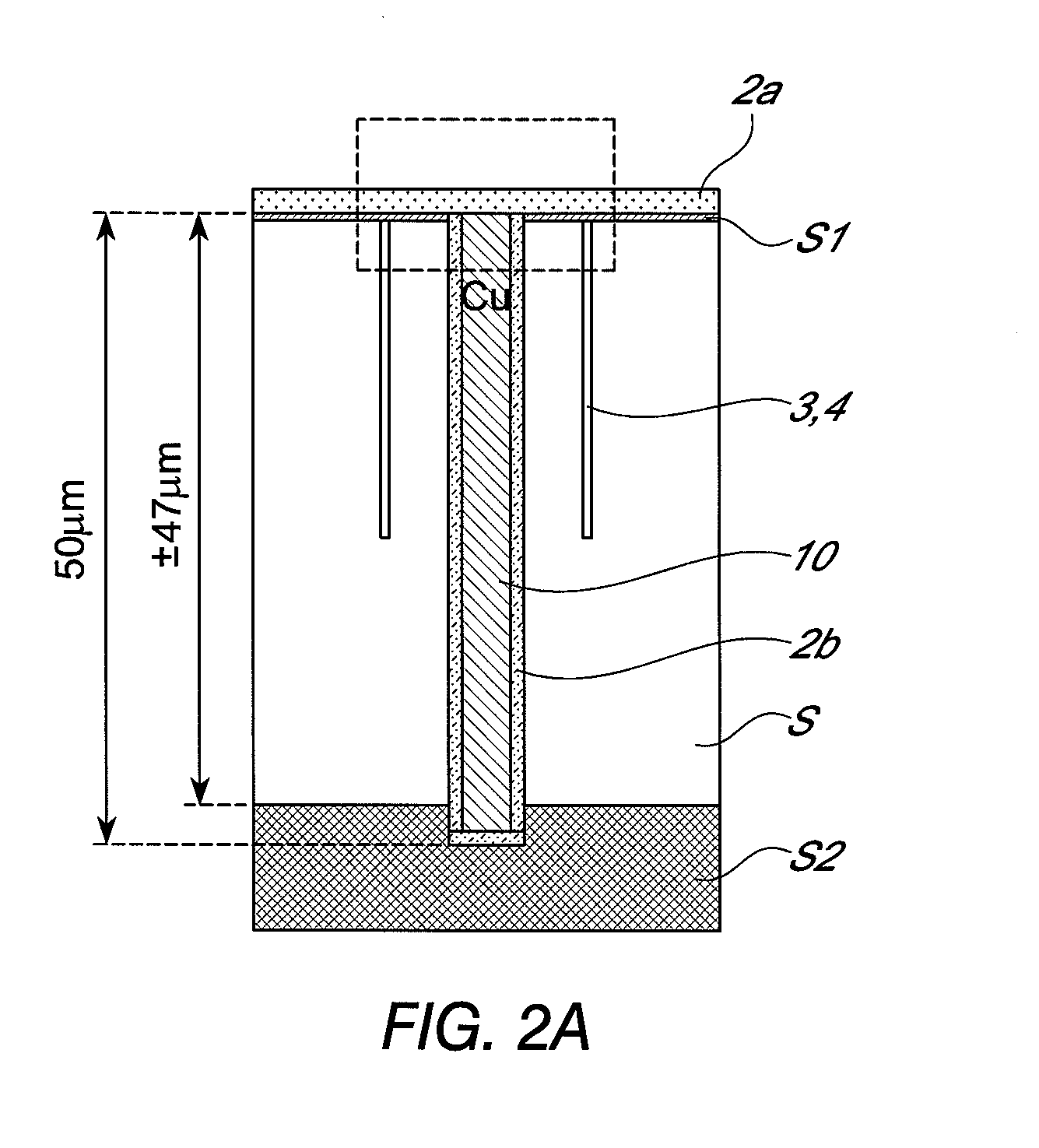
[0048]The present invention will be described with respect to particular embodiments and with reference to certain drawings but the invention is not limited thereto but only by the claims. The drawings described are only schematic and are non-limiting. In the drawings, the size of some of the elements may be exaggerated and not drawn on scale for illustrative purposes. The dimensions and the relative dimensions do not correspond to actual reductions to practice of the invention.

[0049]Furthermore, the terms first, second and the like in the description and in the claims, are used for distinguishing between similar elements and not necessarily for describing a sequence, either temporally, spatially, in ranking or in any other manner. It is to be understood that the terms so used are interchangeable under appropriate circumstances and that the various embodiments described herein are capable of operation in other sequences than described or illustrated herein.

[0050]Moreover, the terms ...


PUM


Abstract

A method is provided for forming at least one TSV interconnect structure surrounded by at least one isolating trench-like structure having at least one airgap. The method comprises at least the steps of providing a substrate having a first main surface and producing simultaneous at least one a TSV hole and a trench-like structure surrounding the TSV hole and separated by remaining substrate material. The method also comprises thereafter depositing a dielectric liner in order to smoothen the sidewalls of the etched TSV hole and to pinch-off the opening of the trench-like structure at the first main surface of the substrate in order to create at least one airgap in said trench-like structure and depositing a conductive material in said TSV hole in order to create a TSV interconnect. A corresponding substrate is also provided.

Description

CROSS-REFERENCE TO RELATED APPLICATIONS[0001]This application claims the benefit under 35 U.S.C. §119(e) of U.S. provisional application Ser. No. 61 / 420,653, filed Dec. 7, 2010, the disclosure of which is hereby expressly incorporated by reference in its entirety and is hereby expressly made a portion of this application.FIELD OF THE INVENTION[0002]Electrical connections in semiconductor devices are provided. More particularly, methods are provided for forming isolation trenches comprising airgaps and interconnect structures such as Through Silicon Vias (TSV) to be used in the stacking of semiconductor devices. The embodiments further relate to devices thus obtained.BACKGROUND OF THE INVENTION[0003]With the continued scaling of IC technology, due to the large amount of electronic circuits on a small area, the density of chip input / output connection pads (I / O's) continues to increase. This leads to an increasing bandwidth of interconnects between integrated circuits (IC's) and / or oth...

Claims


Application Information

Patent Timeline
IPC IPC(8): H01L23/48H01L21/768
CPCH01L21/764H01L21/76898H01L23/481H01L2924/12044H01L2224/13025H01L2224/131H01L2924/13091H01L2924/014H01L2924/00H01L21/7682
Inventor BEYNE, ERIC
Owner INTERUNIVERSITAIR MICRO ELECTRONICS CENT (IMEC VZW)
Why Eureka
Try Eureka