Chucking device and chucking method

a technology of chucking device and chucking method, which is applied in the direction of chucks, mechanical equipment, manufacturing tools, etc., can solve the problems of difficult marked and deviating from the point of contact of the semiconductor substrate surface with each protruding portion, so as to prevent foreign objects from being caught, reduce the difficulty of chucking or conveying a thinner semiconductor substrate, and eliminate the warpage of semiconductor substra

Inactive Publication Date: 2012-06-07
FUJI ELECTRIC CO LTD
View PDF31 Cites 35 Cited by
  • Summary
  • Abstract
  • Description
  • Claims
  • Application Information

AI Technical Summary

Benefits of technology

[0062]Also, according to the nineteenth and twentieth aspects of the invention, the plural suction holes are vacuum drawn at differing timings, thereby chucking the semiconductor substrate to the plural suction holes. Because of this, when holding a semiconductor substrate warped convexly or concavely on the front surface side, it is possible to vacuum draw the plural suction holes in accordance with the warpage of the semiconductor substrate. Consequently, it is possible to hold the semiconductor substrate while eliminating the warpage of the semiconductor substrate.
[0063]Also, according to the twenty-fourth aspect of the invention, after the flow velocity of the gas on the base portion side of the semiconductor substrate is made greater than the flow velocity of the gas on the side opposite to the base portion side of the semiconductor substrate, the plural suction holes are vacuum drawn, thereby chucking the semiconductor substrate to the plural suction holes. Because of this, it is possible to exert a negative pressure caused by a Bernoulli effect on the semiconductor substrate, and hold the semiconductor substrate after placing the semiconductor substrate on the protruding portions in a condition in which the flatness of the semiconductor substrate is increased.
[0064]According to the chucking device and chucking method according to the invention, an effect is achieved whereby it is possible to prevent a foreign object being caught between the device and a semiconductor substrate. Also, an effect is achieved whereby it is possible to hold the semiconductor substrate in a condition in which the semiconductor substrate flatness is maintained or increased.

Problems solved by technology

Also, with the pin chuck type chucking device, a problem occurs in that, due to the sagging of the semiconductor substrate between the protruding portions, the position of the point of contact of the semiconductor substrate surface with each protruding portion deviates more (hereafter referred to as wafer distortion) in comparison with a case of placing the semiconductor substrate on the protruding portions without vacuum drawing.
However, when a semiconductor substrate with a diameter of eight inches is reduced to a thickness of in the region of 60 μm in the manufacturing step of a power semiconductor device such as an IGBT, the warpage of the semiconductor substrate increases markedly.
Because of this, with the kinds of technology shown in the heretofore described patent documents, it is difficult to chuck or convey a thinner semiconductor substrate or markedly warped semiconductor substrate in a condition in which the flatness of the semiconductor substrate is maintained or increased.
However, as heretofore described, the IGBT power semiconductor device warpage is large, for example, in the case of an eight inch diameter semiconductor substrate, it is not unusual that the semiconductor substrate warpage exceeds 1 mm.
When the interval between adjacent protruding portions is approximately 0.7 mm or less when forming quadrangular pyramidic protruding portions on the base portion using an anisotropic etching, the width of an opening portion of a mask covering a region of the base portion that is not etched is too small, and it is difficult to control the amount removed by etching in the crystal plane orientation.
Because of this, controllability of the heights of the protruding portions and the interval between adjacent protruding portions is lost.

Method used


Image

  • Chucking device and chucking method
  • Chucking device and chucking method
  • Chucking device and chucking method

Examples


first embodiment

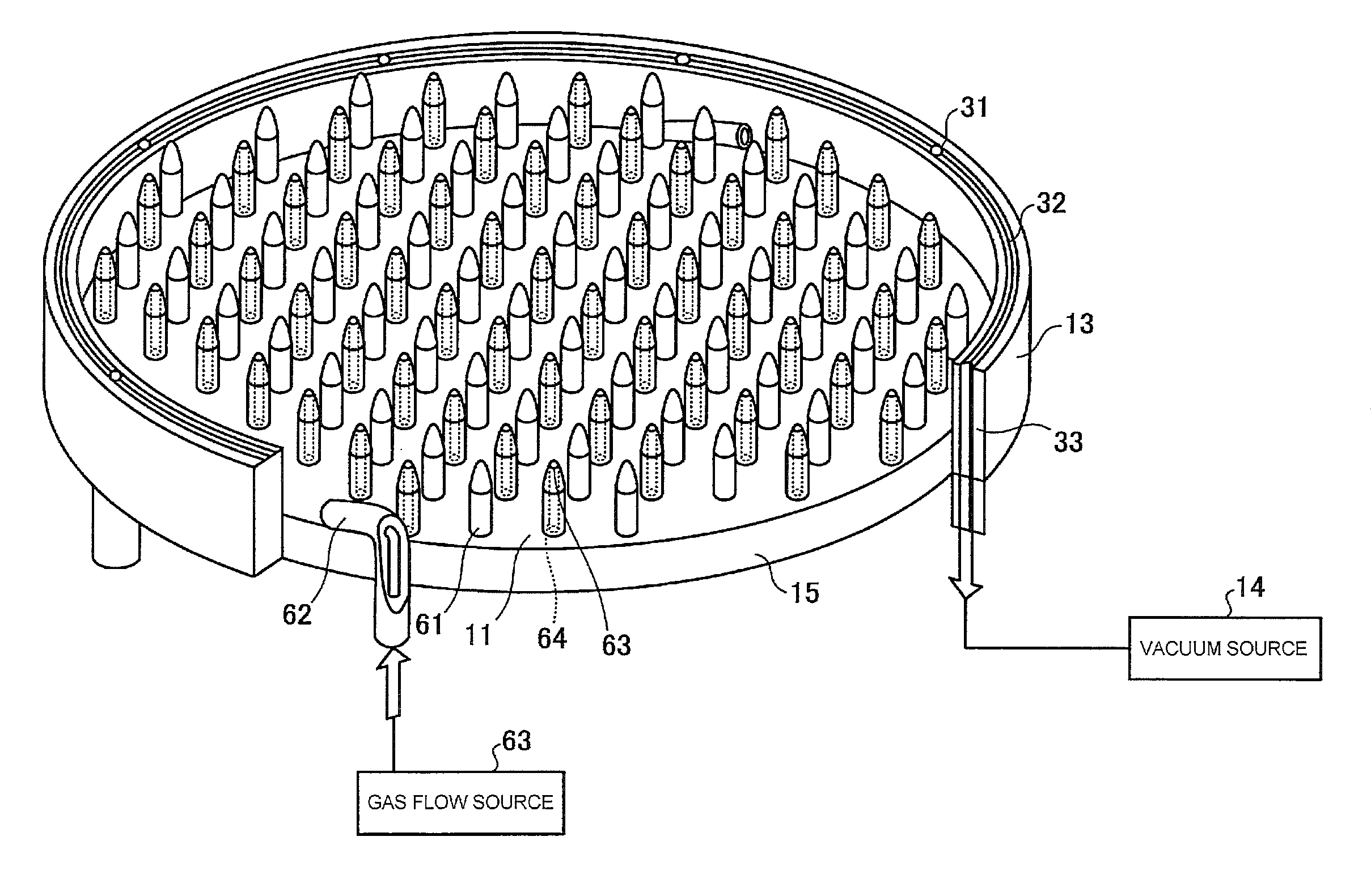
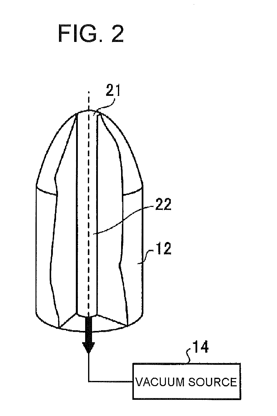
[0088]FIG. 1 is an illustration schematically showing a chucking device according to a first embodiment. Also, FIGS. 2 and 3 are illustrations schematically showing parts configuring the chucking device shown in FIG. 1. The chucking device shown in FIG. 1 includes a base portion 11 on which are provided a plurality of protruding portions 12 that support the central portion of a semiconductor substrate, a cylindrical peripheral portion 13 that supports the outer peripheral portion of the semiconductor substrate, a plurality of suction holes 21 and 31 that chuck the semiconductor substrate, and a vacuum source 14 that vacuum draws (e.g., produces a vacuum in) the plurality of suction holes at differing timings.

[0089]The base portion 11 has, for example, a circular planar shape. The diameter of the base portion 11 is a diameter slightly smaller than the diameter of the semiconductor substrate. Also, the base portion 11 may be configured of a material that has aluminum as a main compone...

second embodiment

[0140]FIG. 11 is an illustration showing a chucking method using a chucking device according to a second embodiment. In the first embodiment, a semiconductor substrate (hereafter referred to as a rib wafer) 51, which has a stepped form owing to a peripheral portion 52 left thickly around the outer perimeter, may be chucked.

[0141]In the second embodiment, as shown in FIG. 11, only a depressed portion farther to the interior than the peripheral portion52 on a main surface side of the rib wafer 51, which has a stepped form owing to the peripheral portion 52, is chucked to the first suction holes 21 provided in the protruding portions 12 and the second suction holes 31 provided in the peripheral portion 13. Also, the heights h of the protruding portions 12 may be made higher than the height of the peripheral portion 13, and the depressed portion of the rib wafer 51, which is thinner owing to the peripheral portion 52, chucked to only the first suction holes 21 provided in the protruding...

third embodiment

[0143]FIGS. 12 and 13 are illustrations showing a chucking method using a chucking device according to a third embodiment. In the first embodiment, a peripheral portion 53 may be provided in such a way as to be able to rise and descend in a vertical direction with respect to the surface of a semiconductor substrate supported on the peripheral portion 53.

[0144]A description will be given of the chucking method of the third embodiment with a case of, for example, chucking the rear surface side of a semiconductor substrate warped concavely on the front surface side as an example. Firstly, using a conveyor arm (not shown) or the like, the semiconductor substrate 1 is placed with the rear surface facing down on the peripheral portion 53 installed in such a way as to be able to rise and descend above the base portion 11, as shown in FIG. 12. Next, a second step is carried out, chucking the outer peripheral portion of the rear surface of the semiconductor substrate 1 to the second suction ...


PUM

PropertyMeasurementUnit
thicknessaaaaaaaaaa
thicknessaaaaaaaaaa
thicknessaaaaaaaaaa

Abstract

A chucking device is disclosed. The chucking device includes plural protruding portions that support the central portion of a semiconductor substrate and that are provided on a base portion. The chucking device also includes a cylindrical peripheral portion that supports the outer peripheral portion of the semiconductor substrate, plural suction holes that chuck the semiconductor substrate, and a vacuum source that vacuum draws the plural suction holes at differing timings. A plurality of mutually independent vacuum drawable suction holes are provided in at least one portion of the protruding portions.

Description

CROSS REFERENCE TO RELATED APPLICATION[0001]The entire disclosure of the inventor's corresponding Japanese patent application, Serial No. JP PA 2010-269819, filed Dec. 2, 2010, is hereby incorporated by reference.BACKGROUND OF THE INVENTION[0002]1. Technical Field[0003]The present invention relates to a chucking device and chucking method.[0004]2. Related Art[0005]In recent years, the importance of a power semiconductor device such as an insulated gate bipolar transistor (IGBT) or insulated gate type field effect transistor (MOSFET) as an environment-adaptive electronic device is increasing. A chucking device that holds a semiconductor substrate by vacuum chucking has been proposed in order to convey a semiconductor substrate along a manufacturing line, or fix the semiconductor substrate to a support stand, in the manufacturing step of the semiconductor device.[0006]FIG. 20 is an illustration showing a heretofore known chucking device. The chucking device shown in FIG. 20 includes a...

Claims


Application Information

Patent Timeline
Patent Type & Authority Applications(United States)
IPC IPC(8): H01L21/687B23B31/30
CPCB25B11/005H01L21/6838Y10T279/11Y10T29/49998H01L21/6875Y10T29/53191
Inventor OOI, HIROYUKI
Owner FUJI ELECTRIC CO LTD
Why Eureka
Try Eureka