Wafer Level Structures and Methods for Fabricating and Packaging MEMS

a technology of actuators and sensors, applied in the field of microelectromechanical systems, can solve the problems of expensive calibration and compensation techniques, cmos ic and mems, and neither the satisfaction of hybrid cmos/mems

Active Publication Date: 2012-06-07
INTEGRATED BIOSENSING TECH
View PDF5 Cites 132 Cited by
  • Summary
  • Abstract
  • Description
  • Claims
  • Application Information

AI Technical Summary

Problems solved by technology

Although both approaches can provide hybrid CMOS / MEMS neither are wholly satisfactory.
In particular, integrally forming the CMOS IC and MEMS on a shared silicon substrate is problematic as the thin film functional layers of the MEMS tend to have thermal properties incompatible with those of the CMOS IC, and as a result require expensive calibration and compensation techniques, or large yield loss of the CMOS due to damage caused during processing.
In addition, because the MEMS is not covered and protected at the wafer or substrate level, there is substantial risk of damaging the MEMS during fabrication of the CMOS IC and / or during die singulation.
Bonding the MEMS substrate over a cavity formed in the CMOS IC substrate is problematic in that the cavity wastes CMOS silicon area and the wet etch or deep reactive ion etch (DRIE) commonly used to form the cavity could damage CMOS circuitry (e.g., electrostatic damage, overheating damage), lowering the yield.
Moreover, the MEMS substrate and CMOS IC substrate are bonded using processes that requires expensive equipment, is difficult to control, and often results in incomplete die bond formation across wafer including center or edge effects, lowering bonding yield.
In addition, these bonding processes are generally non-compatible with typical CMOS foundry processes, and exposing pads on the CMOS IC requires either sawing or mechanical removal of excess silicon, hence lowering yield.

Method used


Image

  • Wafer Level Structures and Methods for Fabricating and Packaging MEMS
  • Wafer Level Structures and Methods for Fabricating and Packaging MEMS
  • Wafer Level Structures and Methods for Fabricating and Packaging MEMS

Examples


first embodiment

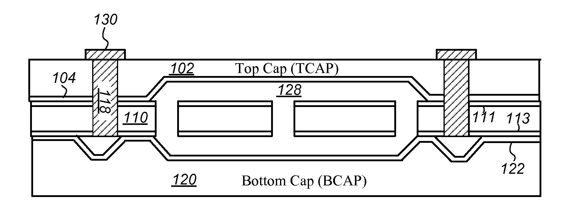
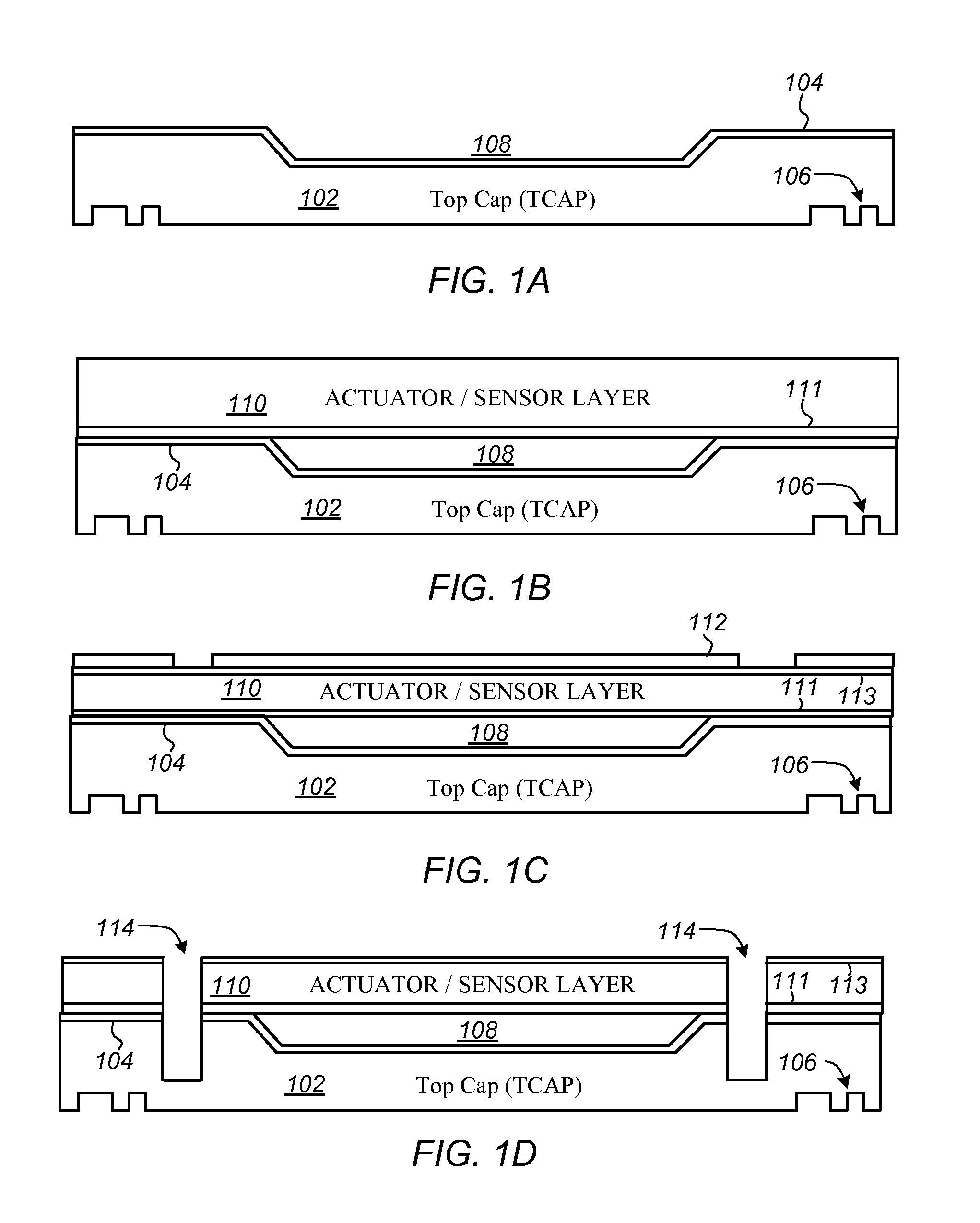
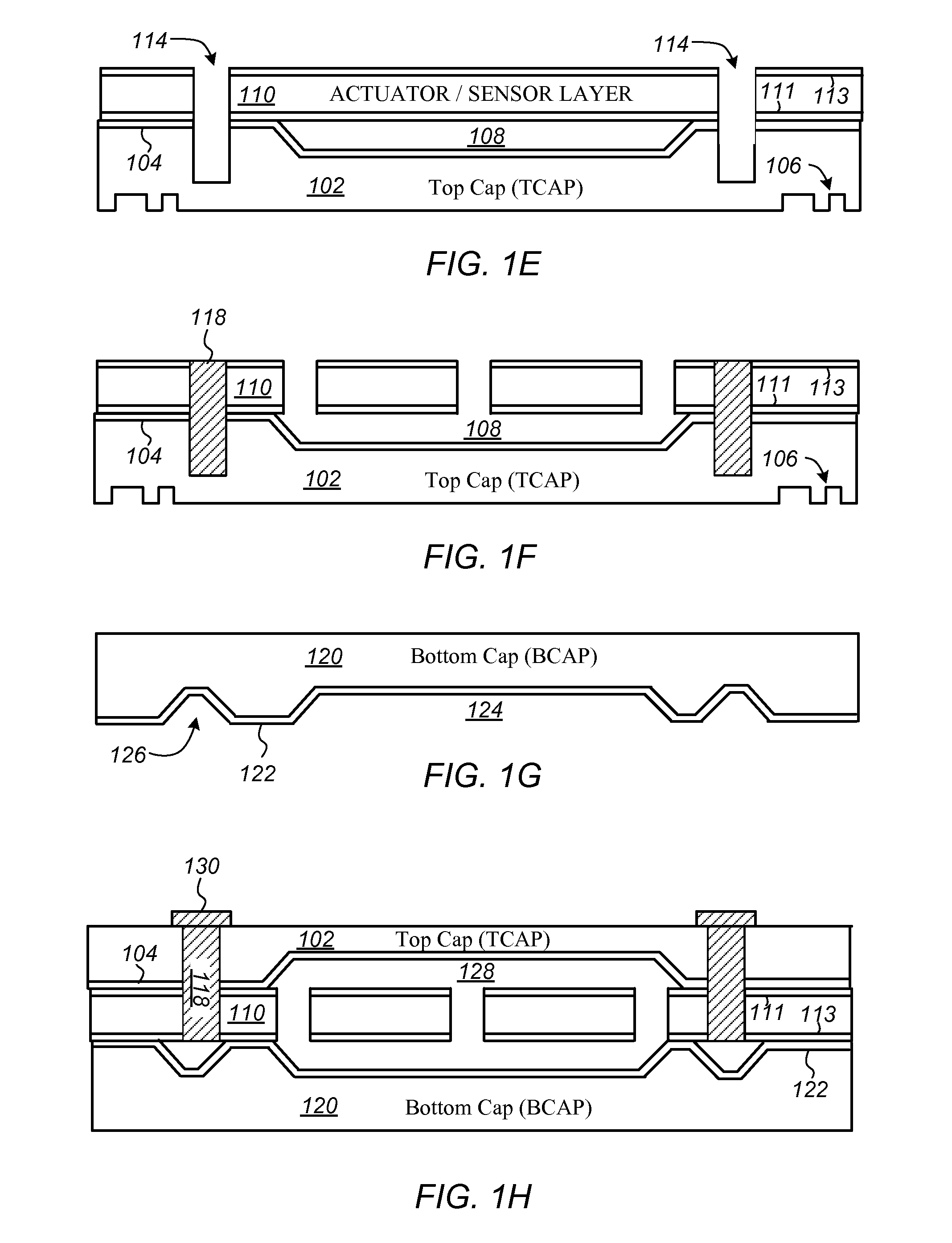
[0033]Referring to FIG. 3A, in a first embodiment the TASP™ or MEMS 300 includes a top cap 302 bonded to an actuator / sensor layer 304 using a bonding material 306, and a bottom cap 308 also bonded to the actuator / sensor layer using a bonding material 310 to form a hermetically sealed cavity 312 around a MEMS actuator or sensor at a wafer or substrate level. The MEMS 300 further includes silicon vias 314. In the embodiment shown, the silicon vias 314 do not extend fully gone thru the actuator / sensor layer 304, but rather stop on or in the actuator / sensor layer making electrical contact from the ball to the actuator layer. This can be accomplished by etching the silicon vias 314 from a top surface 316 of the top cap 302 to or partially into the actuator / sensor layer 304 bonded Thereto. It will be understood that MEMS can be fabricated up to this point by the method similar to that outlined in blocks 200 to 218 of FIG. 2 and described above. The structure of the MEMS 300 further differ...

second embodiment

[0034]Referring to FIG. 3B, in a second embodiment the TASP™ or MEMS 300 includes a top cap 302 bonded to an actuator / sensor layer 304 using a bonding material 306, and a bottom cap 308 also bonded to the actuator / sensor layer using a bonding material 310 to form a hermetically sealed cavity 312 around a MEMS actuator or sensor at a wafer or substrate level. The MEMS 300 further includes silicon vias 314, but differs from that of FIG. 1H in that the silicon vias 314 extend from the actuator / sensor layer 304 through the bottom cap 308 and electrically couple to pads 320 formed on a lower surface of the bottom cap.

[0035]Another method of fabricating and packaging a TASP™ or MEMS according to an alternative embodiment will now be described with reference to the block diagrams of FIGS. 4A-4J, and the flow chart of FIG. 5.

[0036]Referring to FIG. 4A and FIG. 5, the method begins with depositing directly on a first substrate 402 or on an insulating or dielectric material 403, such as silic...

third embodiment

[0057]Referring to FIG. 9C, in a third embodiment the MEMS 902 is directly electrically coupled and attached by WLCSP (wafer level chip-scale-package) solder balls 910 to the CMOS IC 904, which is electrically coupled and attached by wire-bonds 906 to the back-plane 908 in the QFN package.


PUM


Abstract

Methods of fabricating a Micro-Electromechanical System (MEMS) in a hermetically sealed cavity formed at a substrate level are provided. Generally, the method comprises: (i) forming a number of first open cavities in a surface of a first substrate and a number of second open cavities in a surface of a second substrate corresponding to the first open cavities; (ii) forming an actuator/sensor layer including a number of MEMS devices with electrically conductive regions therein; (iii) bonding the first substrate and the second substrate to the actuator/sensor layer so that at least one of the number of the first and second open cavities align with at least one of the number of MEMS devices to form a sealed cavity around the MEMS; and (iv) electrically connecting the electrically conductive regions of the MEMS device to a pad outside of the sealed cavity through an electrical interconnect. Other embodiments are also described.

Description

CROSS-REFERENCE TO RELATED APPLICATIONS[0001]The present application claims the benefit of priority under 35 U.S.C. 119(e) to U.S. Provisional Patent Application Ser. No. 61 / 419,670 entitled “Wafer Level Methods and Structures for Fabricating and Packaging MEMS,” filed Dec. 3, 2010, which application is hereby incorporated by reference in its entirety.TECHNICAL FIELD[0002]The present invention relates generally to Micro-Electromechanical Systems (MEMS), and more particularly to wafer level methods and structures for fabricating and packaging MEMS actuators and / or sensors.BACKGROUND[0003]MEMS have been developed for numerous applications, including sensors such as accelerometers, gyroscopes, pressure sensors, and magnetic sensors, actuators such as atomic force microscopy (AFM) probe tips, micro mirrors, energy harvesters, resonators, motors, and passive programmable components such as Variable Capacitors, Inductors, Resistors, and RF switches or resonators. Typically, the MEMS is el...

Claims


Application Information

Patent Timeline
Patent Type & Authority Applications(United States)
IPC IPC(8): H01L21/56H01L21/78
CPCB81B7/007B81C1/0023B81B2207/097B81B2207/095B81B2207/096B81B2207/092H01L2224/16225H01L2224/32145H01L2224/48091H01L2224/48137H01L2224/48145H01L2224/73265H01L2924/00014H01L2924/00H01L2924/00012
Inventor TAHERI, BABAK
Owner INTEGRATED BIOSENSING TECH
Why Eureka
Try Eureka