Semiconductor memory device and method of operating the same

Active Publication Date: 2012-06-21
SAMSUNG ELECTRONICS CO LTD
View PDF4 Cites 47 Cited by
  • Summary
  • Abstract
  • Description
  • Claims
  • Application Information

AI Technical Summary

Benefits of technology

[0022]In one embodiments, the inventive concept provides a semiconductor memory device comprising; a memory cell array including a plurality of memory strings, each memory string including memory cells series-connected between a string select transistor and a ground select transistor, wherein the round select transistor is connected to a common source line (CSL), a plurality of word lines including a selected word line, wherein the selected word line is commonly connected to gates of a row of memory cells extending across the plurality of memory strings, a plurality of bit lines including a selected bit line, wherein each one of the plurality of bit lines is connected to a corresponding one of the plurality of memory strings, a page buffer that provides output data from selected memory cells associated with at least one of the selected word line and the selected bit line during a verify read operation, a fail bit counter that determines a number of fail cells among the selected memory cells, a voltage controller that generates a read voltage applied to the selected word line during the verify read operation and a pre-charge voltage applied to selected bit line during the read verify operation, and a control circuit that controls the voltage controller in response to the number of fail cells.
[0023]In another embodiment, the inventive concept provides a method of operating a semiconductor memory device comprises; during a program verification operation, applying a read voltage to a selected word line and applying a pre-charge voltage to a selected bit line, and providing output data in response to the read voltage and pre-charge voltage, determining a number of fail cells in view of the output data, wherei

Problems solved by technology

As a result, the threshold voltage of the selected memory cell may unintentionally change.
As a result, it becomes difficult if not impossible to correctly determine whether the memory cell MCc is an OFF-cell, despite its (intended) programmed data state of “0”.
That is,

Method used


Image

  • Semiconductor memory device and method of operating the same
  • Semiconductor memory device and method of operating the same
  • Semiconductor memory device and method of operating the same

Examples


Embodiment Construction

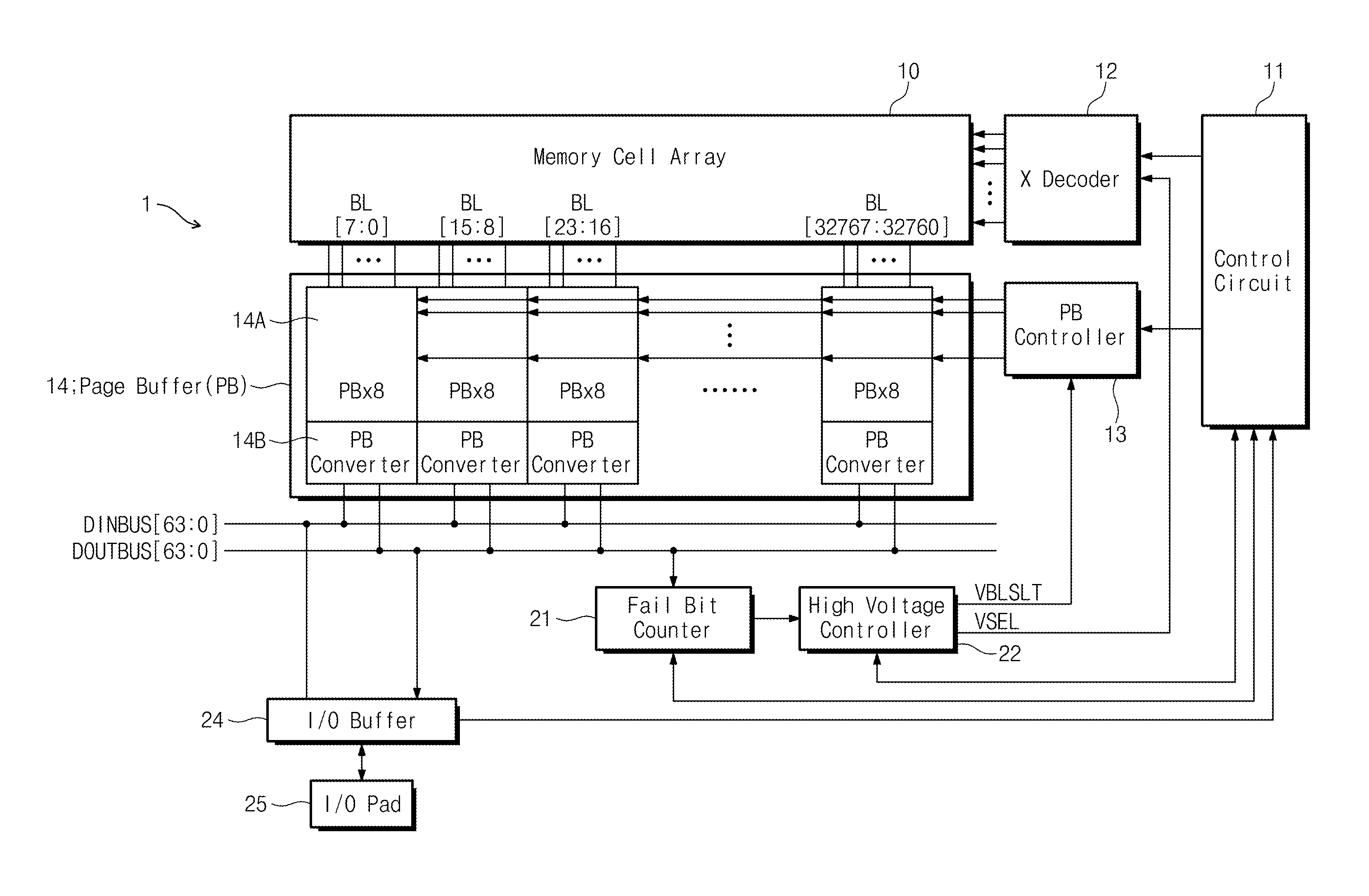
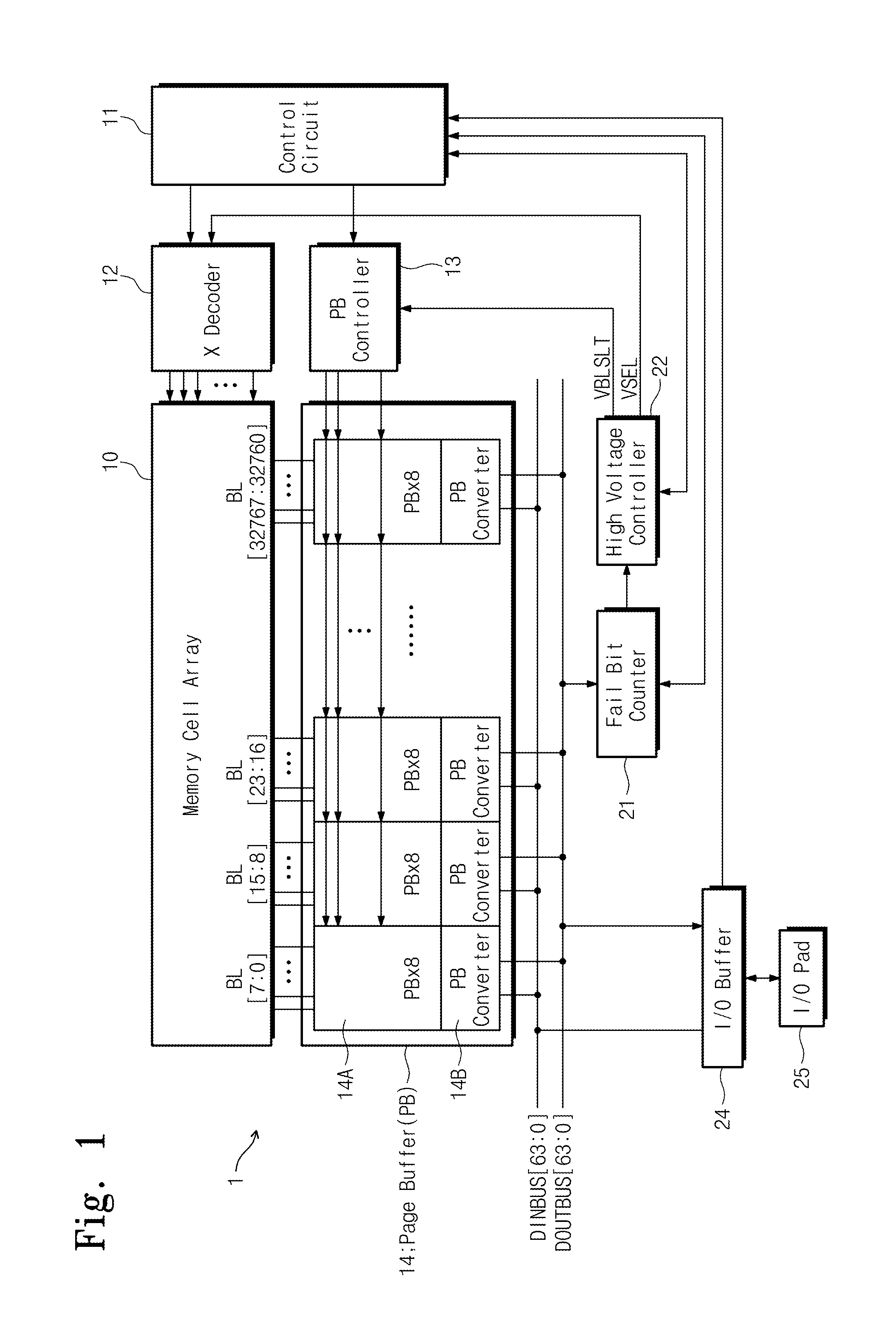
[0039]Embodiments of inventive concepts will be described more fully hereinafter with reference to the accompanying drawings. This inventive concept may, however, be embodied in many different forms and should not be construed as being limited to only the illustrated embodiments. Rather, these embodiments are provided so that this disclosure will be thorough and complete, and will fully convey the scope of the inventive concept to those skilled in the art. Throughout the written description and drawings, like reference numbers and labels refer to like or similar elements.

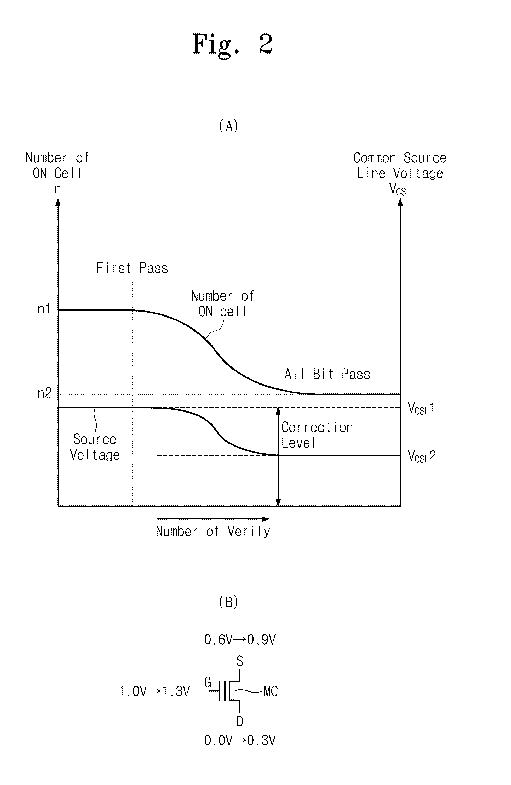
[0040]During a write (or program) operation directed to a selected memory cell in a NAND type flash memory device, data is programmed using an incrementally increasing program voltage over a sequence of programming loops, a program verification operation (a “verify read operation”) associated with each loop is typically required to carefully control the resulting threshold voltage distribution of the selected memory...


PUM


Abstract

A semiconductor memory device operate during a program verification operation to apply a read voltage to a word line and a pre-charge voltage to a bit line in order to provide output data. A number of fail cells is determined in view of the output data, wherein the number of fail cells is directly related to an increase in voltage on a common source line (CSL) connected to memory cells providing the output data. During a subsequent program verification operation, the level of at least one of the read voltage and the pre-charge voltage is adjusted in response to the number of fail cells.

Description

CROSS-REFERENCE TO RELATED APPLICATIONS[0001]This U.S. non-provisional patent application claims priority under 35 U.S.C. §119 to Japanese Patent Application No. 2010-0283607 filed on Dec. 20, 2010, the subject matter of which is hereby incorporated by reference.BACKGROUND OF THE INVENTION[0002]The present inventive concept relates to semiconductor memory devices and methods of operating the same.[0003]Nonvolatile memory devices have the capability of retaining stored data in the absence of applied power. There are different types of nonvolatile memory devices. However, so-called flash memory, including several types of electrically erasable nonvolatile memory, has become an important component of many contemporary digital data and consumer electronics devices. NAND type flash memory is configured using a plurality of memory strings, wherein each memory string includes a plurality of series-connected memory cells arranged between intersecting bit lines and word lines.[0004]Figure (F...

Claims


Application Information

Patent Timeline
IPC IPC(8): G11C16/26
CPCG11C16/3459G11C16/0483G11C16/06G11C16/26
Inventor CHOKAN, TOMOHITOSUDOU, NAOAKI
Owner SAMSUNG ELECTRONICS CO LTD
Why Eureka
Try Eureka