Thermal detector, thermal detection device, electronic instrument, and thermal detector manufacturing method

Inactive Publication Date: 2012-06-28
SEIKO EPSON CORP
View PDF1 Cites 26 Cited by
  • Summary
  • Abstract
  • Description
  • Claims
  • Application Information

AI Technical Summary

Problems solved by technology

In addition, with the infrared light detecting element described in Japanese Patent No. 3339276, the infrared light absorbing layer is at a position that is separated from the infrared sensing part heat-detecting element, and so the heat that is generated in the infrared light ab

Method used


Image

  • Thermal detector, thermal detection device, electronic instrument, and thermal detector manufacturing method
  • Thermal detector, thermal detection device, electronic instrument, and thermal detector manufacturing method
  • Thermal detector, thermal detection device, electronic instrument, and thermal detector manufacturing method

Examples


embodiment 1

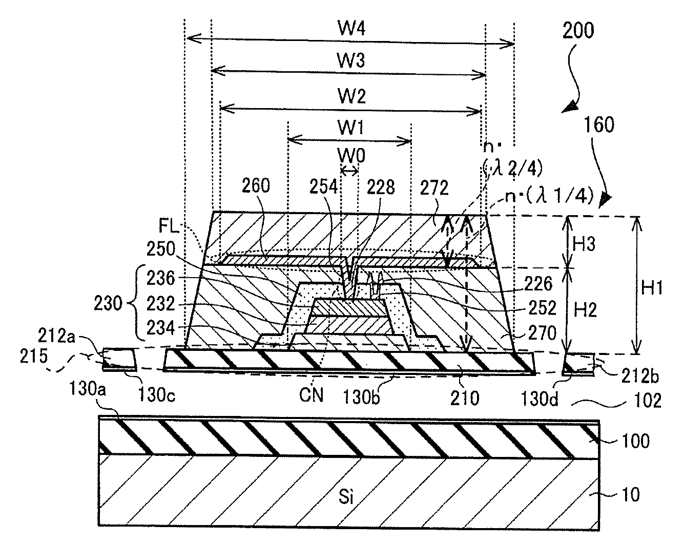
[0086]FIGS. 1A and 1B are plan view and a sectional view of an example of the thermal detector. FIG. 1B is a sectional view of the thermal detector, taken along line A-A′ in FIG. 1A. In FIGS. 1A and 1B, an individual thermal detector is shown, but a plurality of thermal detectors may be disposed in the form of a matrix in order to produce the configuration of a thermal detector array (e.g., a thermal-type detection device).

[0087]The thermal detector shown in FIGS. 1A and 1B is a pyroelectric infrared detector (a type of light sensor) 200 (however, this is only an example and does not limit the invention). This pyroelectric type infrared photodetector 200 can efficiently transfer the heat that is generated by light absorption in the two-layer light-absorbing films 270 and 272 to the heat-detecting element (here, a pyroelectric capacitor 230) via a thermal transfer member 260 having favorable thermal transfer properties.

[0088]The thermal transfer member 260 may be constituted by a mat...

embodiment 2

[0181]The thermal detector manufacturing method of this embodiment is described below with reference to FIGS. 13 to 15. First, FIGS. 13A to 13E will be discussed. FIGS. 13A to 13E are diagrams that show the main steps of the thermal detector manufacturing method up until formation of the first light-absorbing layer.

[0182]In the step shown in FIG. 13A, a silicon substrate (which may have elements such as transistors) is prepared, and a structure 100 including an insulating layer (e.g., a multilayer wiring structure) is formed on the silicon substrate 10. An etching stopper film 130a is then formed on the structure 100 including the insulating layer, and a sacrificial layer (e.g., an SiO2 layer) 101 is then formed.

[0183]In the step of FIG. 13B, an etching stopper film 130b is formed on the sacrificial layer 101. Next, a thick film that will serve as the support member (membrane) 215 (e.g., a thick film composed of a three-layer laminated film) is formed.

[0184]In the step of FIG. 13C, ...

embodiment 3

[0191]FIG. 16 is a diagram showing another example of the thermal detector. With the thermal detector 200 shown in FIG. 16, the cavity 102 is formed for each individual heat-detecting element, and the support member (membrane) 215 is supported by the structure (part of the base part) that surrounds the cavity 102. In addition, a circuit constituent element (in this case, a MOS transistor) is formed in the region overlapping the heat-detecting element as seen in plan view. This MOS transistor is connected via multilayer wiring to the pyroelectric capacitor 230 that is used as the heat-detecting element. In the example of FIG. 16, the thermal transfer member 260 is utilized as wiring.

[0192]Specifically, a source layer (S) and a drain layer (D) are formed in the substrate (silicon substrate) 10. In addition, a gate insulating film INS and a gate electrode G (e.g., a polysilicon gate electrode) are formed on the substrate 10. As a result, a MOS transistor that serves as the circuit cons...


PUM

PropertyMeasurementUnit
Wavelengthaaaaaaaaaa
Lightaaaaaaaaaa

Abstract

A thermal detector includes: a substrate; a support member supported so that a cavity is formed between the substrate and the support member; a heat-detecting element supported on the support member; a thermal transfer member disposed over the heat-detecting element, and including a thermal collecting portion made of a material having light-reflecting characteristics and having a pattern with which a portion of light incident to a region defined by the support member as seen in plan view enters towards the support member, and a connecting portion connecting the thermal collecting portion to the heat-detecting element; a first light-absorbing layer contacting the thermal transfer member between the thermal transfer member and the support member; and a second light-absorbing layer contacting the thermal transfer member and disposed on the thermal transfer member.

Description

CROSS-REFERENCE TO RELATED APPLICATIONS[0001]This application claims priority to Japanese Patent Application No. 2010-286334 filed on Dec. 22, 2010, Japanese Patent Application No. 2010-289491 filed on Dec. 27, 2010, Japanese Patent Application No. 2010-289492 filed on Dec. 27, 2010, Japanese Patent Application No. 2011-012060 filed on Jan. 24, 2011 and Japanese Patent Application No. 2011-036886 filed on Feb. 23, 2011. The entire disclosures of Japanese Patent Application Nos. 2010-286334, 2010-289491, 2010-289492, 2011-012060 and 2011-036886 are hereby incorporated herein by reference.BACKGROUND[0002]1. Technical Field[0003]The present invention relates to a thermal detector, a thermal detection device, an electronic instrument, and a thermal detector manufacturing method.[0004]2. Related Art[0005]Thermal detection devices are known as light sensors. Thermal detectors absorb light that has been emitted from an object in a light-absorbing layer, convert the light to heat, and measu...

Claims


Application Information

Patent Timeline
IPC IPC(8): G01J5/02B05D5/12
CPCG01J5/0225G01J5/024G01J5/025G01J5/0853Y10T29/4981G08B13/19697H01L37/02H01L35/34G01J5/34H10N15/10H10N10/01
Inventor TSUCHIYA, YASUSHI
Owner SEIKO EPSON CORP
Why Eureka
Try Eureka