Method of forming a photonic crystal material

a technology of photonic crystal material and forming method, which is applied in the direction of magnetic recording, spectral modifier, dough sheeter/rolling machine/rolling pin, etc., can solve the problems of reducing or even completely losing the optical effect of the photonic crystal material, reducing the efficiency of production of such films on an industrial scale, and so as to achieve the effect of ensuring the long-term stability of the optical effect, ensuring the long-

Inactive Publication Date: 2012-06-28
DE LA RUE INT LTD
View PDF10 Cites 22 Cited by
  • Summary
  • Abstract
  • Description
  • Claims
  • Application Information

AI Technical Summary

Benefits of technology

[0013]The optical effects of the invention are not intended to be limited to operate only in the wavelengths observable by the human eye. Thus, in addition to visible light it is intended that the invention may be practised at other non-visible wavelengths including ultra-violet and infra-red regimes within the electromagnetic spectrum. One or each of the first and second optical effects may be in the visible or non-visible parts of the spectrum. When the incident light is produced by a white light (broad wavelength band) source, preferably at least the second optical effect is a colour effect. Whilst the first and second effects are preferably observed as reflective effects, transmissive effects are also contemplated.
[0014]With reference to the film itself, typically the film has a maximum dimension in an elongate direction, an intermediate dimension in a width direction that is substantially normal to the elongate direction, and a minimum dimension in a thickness direction that is substantially normal to each of the elongation and width directions. In this case the second optical effect is present across substantially the full width of the film in the width direction. Similarly the second optical effect is present along substantially the full length of the film in the elongate direction, which provides that substantially all of the film area exhibits the second optical effect.
[0015]The film may be produced in batches, in which case each batch may provide a long length of film, for example tens of metres in length. In order to produce the film most efficiently it is preferably produced as a continuous film. For example, provided a supply of materials is assured for generating the film, it may be continuously produced and processed, followed by spooling and cutting downstream, prior to or subsequent to any further processing.
[0016]The method is, in principle, not limited to any particular film thicknesses, although it finds particularly beneficial application where the thickness of the film is 100 micrometres or less. Most preferably the film has a thickness of 40 micrometres or less. Thin films of 100 micrometres or less are particularly beneficial for many security applications since they may be incorporated into documents of value and thereby provide new optical effects which are extremely difficult to counterfeit.
[0017]A number of different techniques may be used for producing the film according to the first process. Where the films are polymeric, the production methods include rolling, calendaring, film blowing or flat-film extrusion.
[0018]In the production of a strong and homogeneous second optical effect it is beneficial to ensure that the film has a smooth surface prior to application of the second process. This may be achieved by performing a calendaring process on the film before performing the second process (and therefore as part of the first process or as an intermediate process). Typically such a calendaring process applies a pressure to the film of between 50 and 200 bar (about 5 to 20 MPa) and at a temperature of 80 to 120 Celsius. Once the film has been processed to produce the second optical effect it is beneficial to ensure the long-term stability of the optical effect. This may be achieved by a process of cross-linking. Such cross-linking may be achieved by the provision of additives within the film material which are responsive to stimulation by heat or ultra-violet light. It is preferred that thermal cross-linking is performed since the second process is typically performed at an elevated temperature which may simplify the processing required. Cross-linking may also be used to reduce any surface stickiness of the films.

Problems solved by technology

However, if the modulation in refractive index is sufficiently strong, propagation of certain frequencies can be forbidden for any crystalline direction, and a complete photonic band gap arises.
Unfortunately a significant problem exists because the fabrication methods inherent within film production are not always amenable to the preservation of the photonic structure of the materials.
The result is that film production techniques cause the reduction or even complete loss of any optical effects exhibited by the photonic crystal material.
Further challenges exist in the production of such films on an industrial scale.
One such challenge is the production of homogeneous optical properties such that all of the film can be observed to produce a similar optical effect.
These can result in films having significant variations in optical properties in different regions, which increases wastage and costs.
Furthermore, other challenges exist in the provision of films which may be readily handled, particularly in the case of films which are thin (for example under 100 micrometres) where the film strength may be low or surface stickiness may prevent ease of use.

Method used


Image

  • Method of forming a photonic crystal material
  • Method of forming a photonic crystal material
  • Method of forming a photonic crystal material

Examples


Embodiment Construction

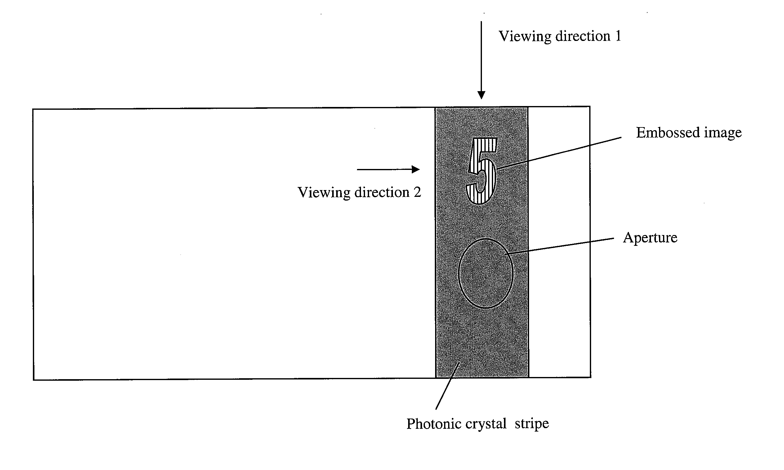
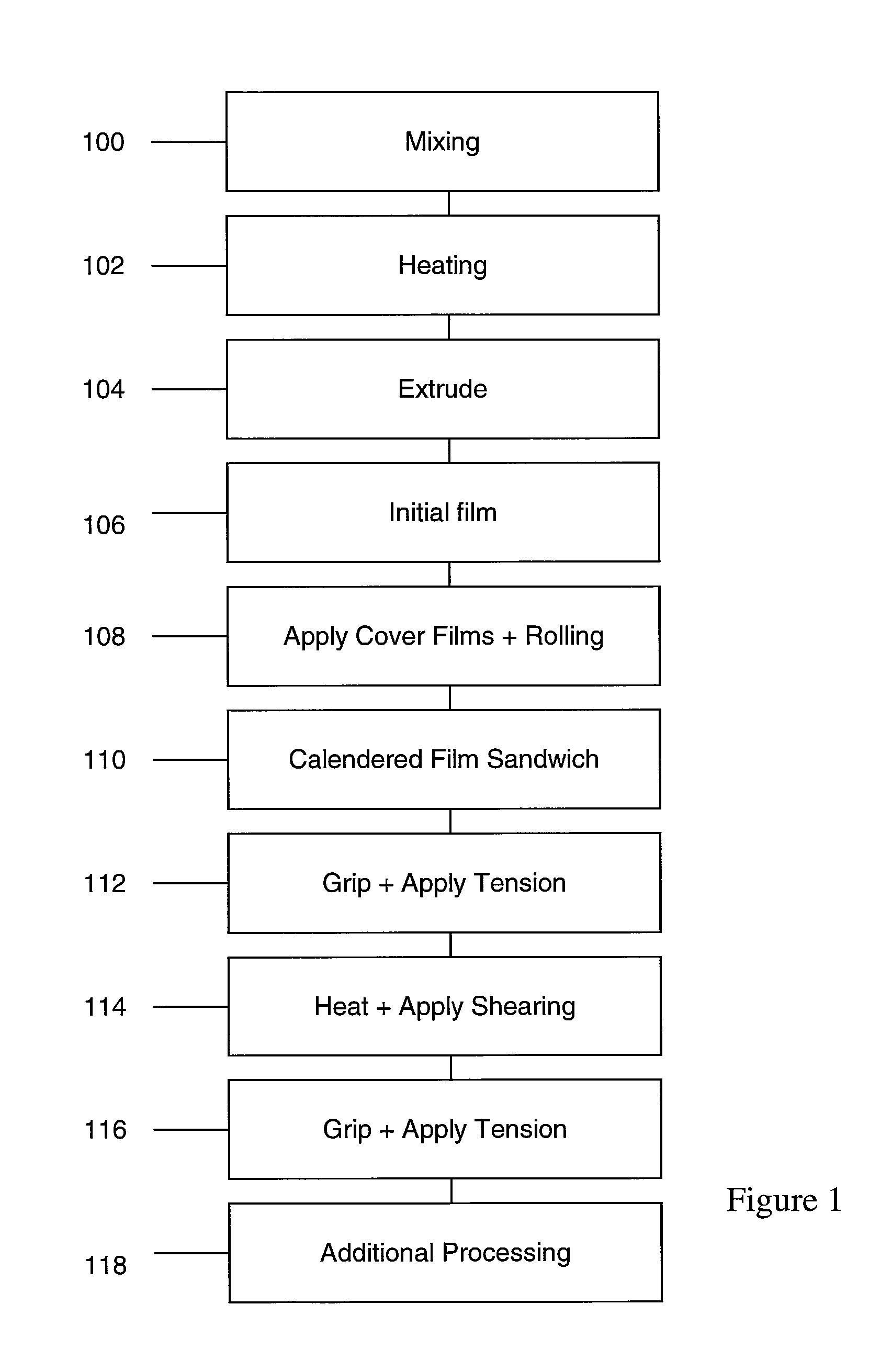
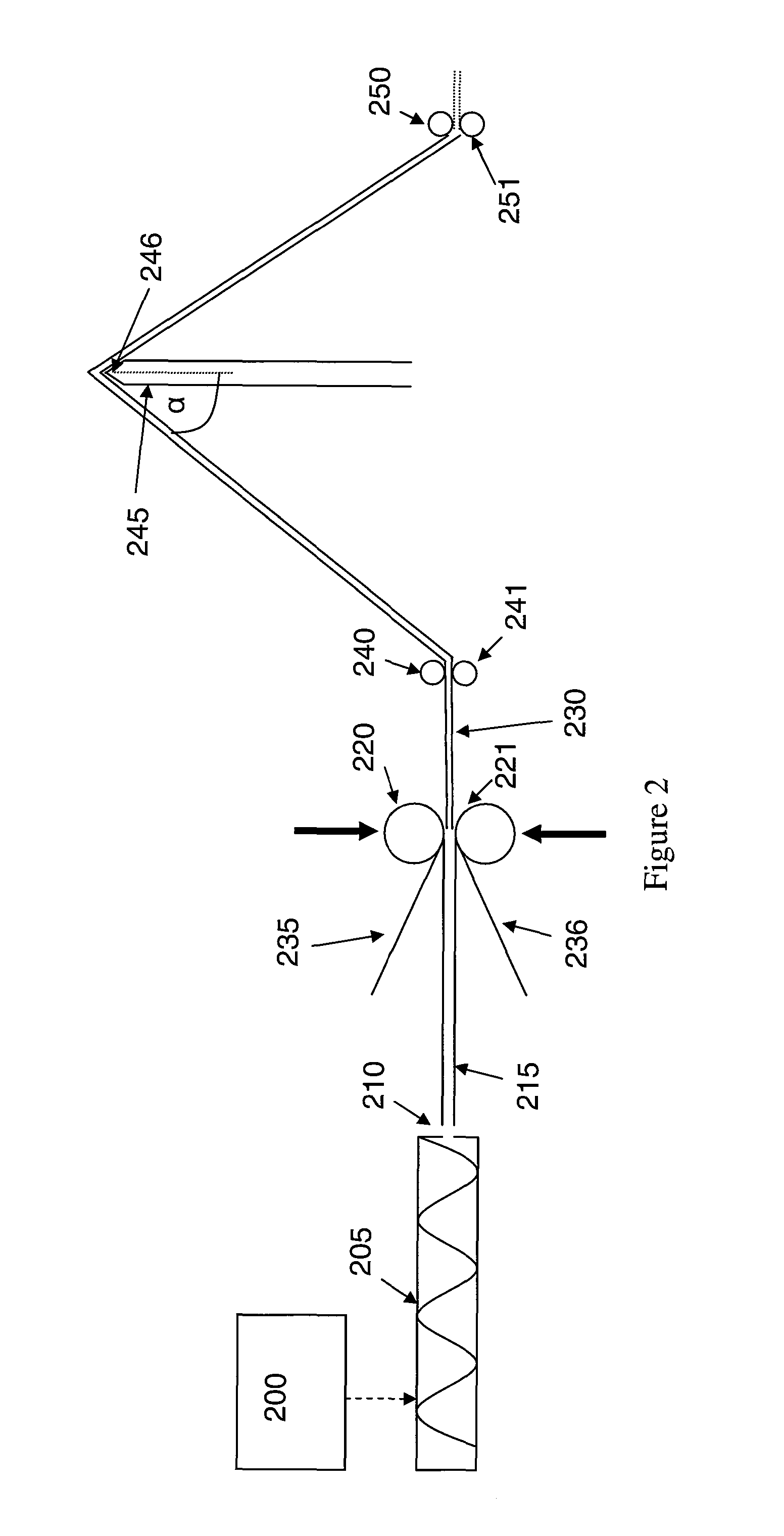
[0072]We now describe a method, together with suitable apparatus, for producing a thin film of photonic crystal material which exhibits a strong angularly dependent colour effect. We then describe the use of the film in various example applications related to security devices and documents.

Materials

[0073]The present invention is not intended to be limited by the specific use of certain materials and this example now illustrates one practical implementation. As has been explained known methods of forming photonic crystal materials include micro fabrication and self-assembly. Due to the complexities of micro fabrication processes, it has become preferred in the art to use self-assembly. Synthetic opal structures can be formed by such a mechanism where uniformly sized sub-micron siliceous spheres are organised through a sedimentation process in a face-centred cubic crystal structure. Likewise, inverse-opal structures can also be formed by the dissolution of the siliceous spheres. Whils...


PUM

PropertyMeasurementUnit
thicknessaaaaaaaaaa
thicknessaaaaaaaaaa
temperatureaaaaaaaaaa

Abstract

A method of forming a film of photonic crystal material. A first process is performed upon a material capable of having a photonic crystal structure, this process causing deformation of the material so as to form a film in which incident light received by the material is selectively reflected or transmitted to generate a first optical effect in the film. A second process is performed upon substantially all of the film which applies a shear stress to the film. This causes a change in the material structure so as to generate a second optical effect in the film, different from the first optical effect, in response to incident light. Security films, devices, articles and documents formed using the method are also discussed.

Description

FIELD OF THE INVENTION[0001]The present invention relates to improvements in methods of forming films of photonic crystal material having an optical effect.BACKGROUND TO THE INVENTION[0002]Photonic crystals are structured optical materials in which the refractive index varies periodically in two or preferably three dimensions. These materials exhibit a range of interesting optical effects when subject to electromagnetic radiation of a wavelength comparable to the spatial modulation of the refractive index. Bragg reflection may occur over a range of wavelengths that depend on the direction of incidence / propagation and the periodicity of refractive index variation. This gives rise to photonic ‘energy gaps’ that are analogous to the electronic band gaps in semiconductors. Typically, electromagnetic waves within a certain frequency range cannot propagate in particular directions within the crystal, and incident electromagnetic radiation at these wavelengths is consequently reflected. It...

Claims


Application Information

Patent Timeline
Patent Type & Authority Applications(United States)
IPC IPC(8): B42D15/00B29C55/02B32B3/00B29C59/00B29C65/00G02B5/23B29D11/00G02B1/02
CPCB29C55/023B29C55/06B29C55/065Y10T428/24355B29K2995/0018B82Y20/00Y10T156/1002B29C55/18
Inventor VULPIUS, GUNTHERHELLMANN, GOTZ PETERSPAHN, PETER WOLFGANG ANDREAS
Owner DE LA RUE INT LTD
Why Eureka
Try Eureka