Multi-chip stack package structure and fabrication method thereof

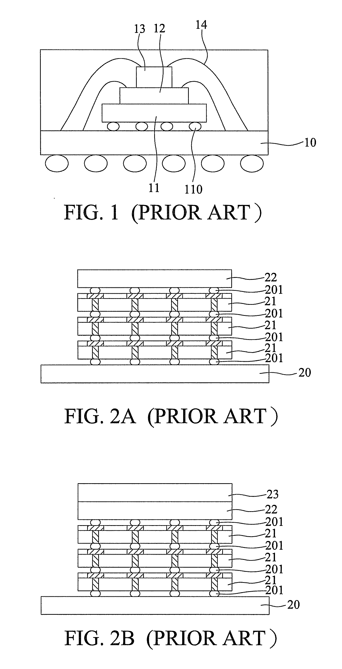
a technology of multi-chip stack and package structure, which is applied in the direction of electrical apparatus, semiconductor devices, semiconductor/solid-state device details, etc., can solve the problems of limiting the number of stacked chips, limiting the electrical functionality, and the number of semiconductor chips that can be horizontally mounted on the packaging substrate is quite limited, so as to avoid the risk of cracking of the multi-chip stack package structure, improve the heat dissipation efficiency, and increase the overall structur

Inactive Publication Date: 2012-07-05
SILICONWARE PRECISION IND CO LTD
View PDF6 Cites 11 Cited by
  • Summary
  • Abstract
  • Description
  • Claims
  • Application Information

AI Technical Summary

Benefits of technology

[0021]Therefore, the multi-chip stack package structure and the fabrication method thereof according to the present invention involve providing an inner-layer heat sink having two opposite surfaces and a plurality of conductive through holes penetrating the two opposite surfaces, disposing at least a chip on each of the two surfaces of the inner-layer heat sink, and electrically connecting the chips to the conductive through holes. As such, the inner-layer heat sink disposed between the chips provides a heat-dissipating path for rapidly dissipating heat generated by chips in the middle of the package structure, thereby eliminating the need to transfer heat from layer to layer and accordingly improving the heat dissipating efficiency. Further, by using a metal plate having an oxide layer as a heat sink, the rigidity of the overall structure is increased so as to avoid the risk of cracking of the multi-chip stack package structure.

Problems solved by technology

However, due to the limited size of the packaging substrate, the number of semiconductor chips that can be horizontally mounted on the packaging substrate is quite limited.
However, to facilitate the process of wire bonding, the second semiconductor chip 12 must be smaller than the first semiconductor chip 11 and the third semiconductor chip 13 must be smaller than the second semiconductor chip 12, thus limiting the number of stacked chips, limiting the electrical functionality and adversely affecting the electrical transmission efficiency of the overall structure.
However, in such a package structure, heat generated by the TSV chips 21 in the middle of the stack structure is not easily dissipated due to the small spacings between the chips, thus adversely affecting the operation of the TSV chips 21 and even causing damage to the TSV chips 21.
However, such a heat dissipating path is rather long, which leads to a low heat dissipating efficiency.
Further, the area of the metal heat sink 23 cannot greatly exceed the area of the semiconductor chip 22 because a too large metal heat sink 23 can cause attaching difficulty and stress problems and even cause cracking of the chip 22.

Method used


Image

  • Multi-chip stack package structure and fabrication method thereof
  • Multi-chip stack package structure and fabrication method thereof
  • Multi-chip stack package structure and fabrication method thereof

Examples


first embodiment

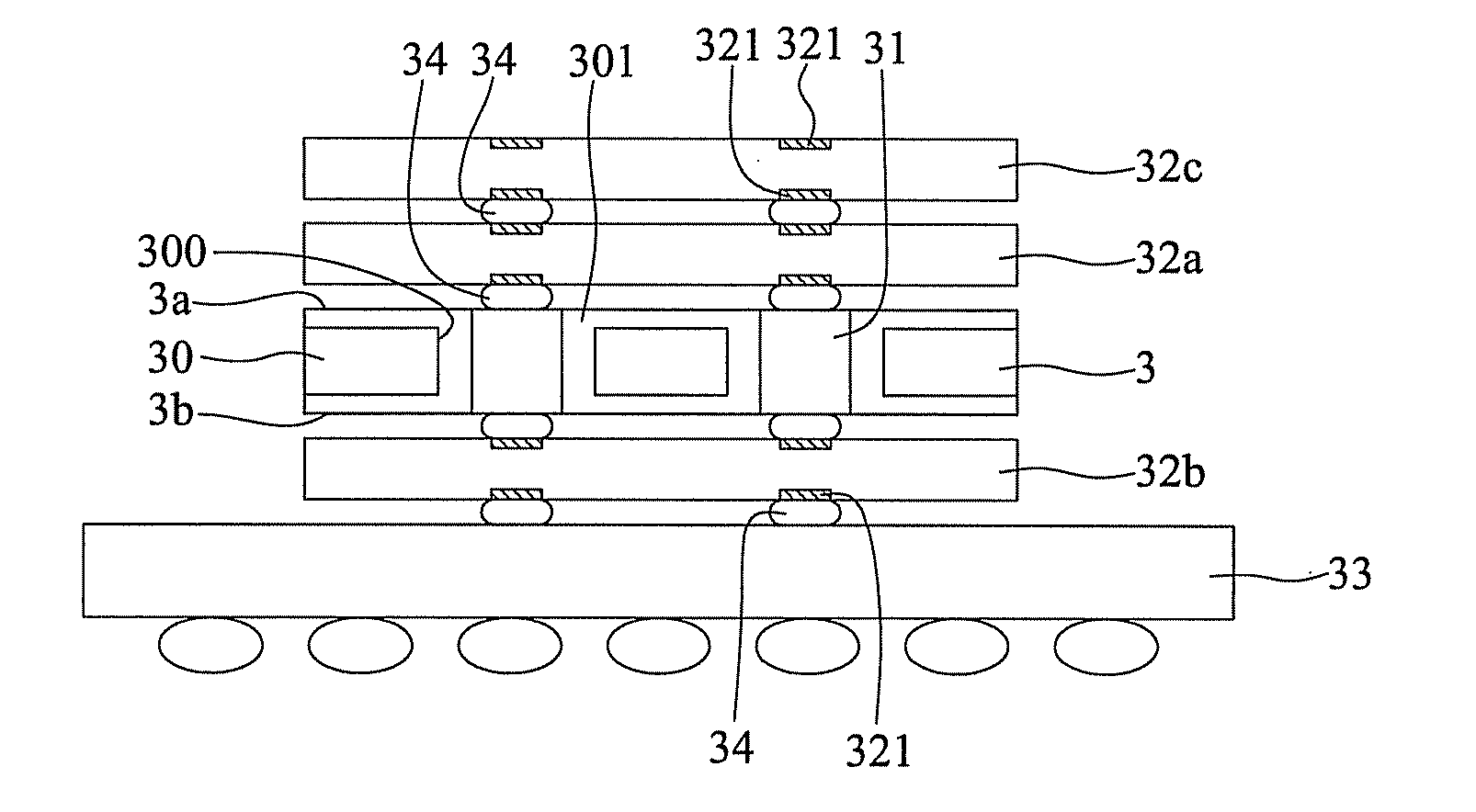
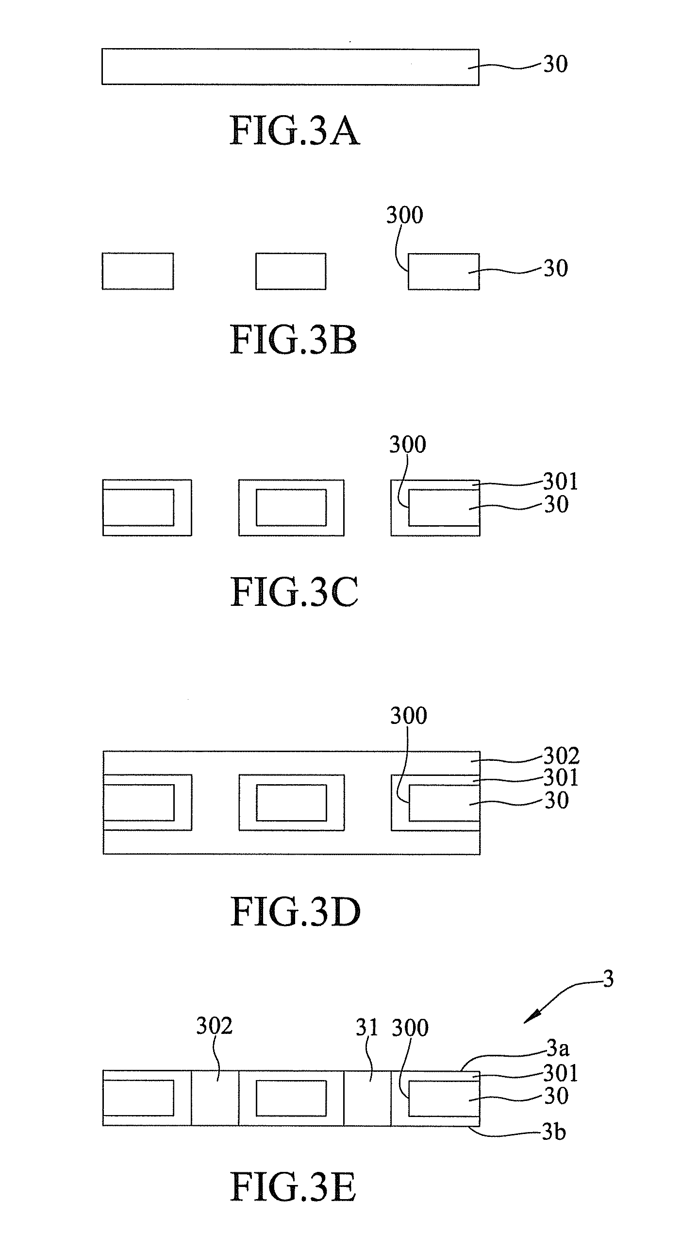
[0028]FIGS. 3A to 3G show a fabrication method of a multi-chip stack package structure according to a first embodiment of the present invention. Therein, FIGS. 3A to 3E show fabrication of an inner-layer heat sink 3 (as shown in FIG3E) having a first surface 3a and a second surface 3b opposite to the first surface 3a and a plurality of conductive through holes 31 penetrating the first surface 3a and the second surface 3b.

[0029]Referring to FIG. 3A, a metal plate 30 madeof, for example, aluminum is provided.

[0030]Referring to FIG. 3B, a plurality of through holes 300 penetrating the metal plate 30 is formed by mechanical drilling or laser drilling

[0031]Referring to FIG. 3C, an oxide layer 301 is formed on the metal plate 30 and on the walls of the through holes 300. The oxide layer 301 is made of, for example, aluminum oxide.

[0032]Referring to FIGS. 3D and 3E, the through holes 300 are filled with a conductive material so as to serve as conductive through holes 31. Referring to FIG....

second embodiment

[0039]FIGS. 4A to 4I show a fabrication method of a multi-chip stack package structure according to a second embodiment of the present invention. In the present embodiment, the planar size of the inner-layer heat sink is larger than the area of the first chip such that a metal cover can be disposed on the inner-layer heat sink.

[0040]FIGS. 4A to 4E show fabrication of the inner-layer heat sink. Referring to FIG. 4A, a metal plate 30 is provided and a plurality of through holes 300 penetrating the metal plate 30 is formed.

[0041]Referring to FIG. 4B, an oxide layer 301 is formed on a portion of the metal plate 30 and on the walls of the through holes 300 such that a portion of the metal plate 30 is exposed for disposing of the metal cover. For example, a resist layer 40 is formed around the periphery of the two opposite surfaces 30a, 30b of the metal plate 30, and openings 400 are formed in the resist layer 40 to expose a portion of the metal plate 30 and the conductive through holes 3...


PUM


Abstract

A multi-chip stack package structure includes: an inner-layer heat sink having a first surface and a second surface opposing one another and having a plurality of conductive vias penetrating the first surface and the second surface; a first chip disposed on the first surface of the inner-layer heat sink; and a second chip disposed on the second surface of the inner-layer heat sink. Thereby, a heat-dissipating path is provided within inner-layers of the multi-chip stack package structure, and the rigidity of the overall structure is enhanced.

Description

BACKGROUND OF THE INVENTION[0001]1. Field of the Invention[0002]The present invention relates to package structures and fabrication methods thereof, and, more particularly, to a multi-chip stack package structure and a fabrication method thereof.[0003]2. Description of Related Art[0004]Electronic products are becoming lighter, thinner, shorter and smaller. Meanwhile, demand continues for electronic products with high efficiency, low power consumption and multi-functionality. To meet such demand, a semiconductor package with a plurality of semiconductor chips horizontally mounted on a packaging substrate has been developed. However, due to the limited size of the packaging substrate, the number of semiconductor chips that can be horizontally mounted on the packaging substrate is quite limited. Accordingly, a multi-chip stack structure has also been developed to reduce the occupied area of the packaging substrate and shorten the transmission path, thereby achieving high efficiency, lo...

Claims


Application Information

Patent Timeline
Patent Type & Authority Applications(United States)
IPC IPC(8): H01L23/498H01L21/56
CPCH01L23/3128H01L23/3677H01L23/4334H01L2224/16145H01L2224/48227H01L25/0657H01L2225/06513H01L2224/06181H01L2224/16225H01L2224/16245H01L2225/06517H01L2225/06589H01L2924/15311H01L2224/0401H01L2224/16235H01L2224/17181
Inventor HUANG, PIN-CHENGCHAO, CHUN-CHIEHCHIU, CHI-HSIN
Owner SILICONWARE PRECISION IND CO LTD
Why Eureka
Try Eureka