Separation of doping density and minority carrier lifetime in photoluminescence measurements on semiconductor materials

Inactive Publication Date: 2012-07-19
BT IMAGING PTY LTD
View PDF1 Cites 22 Cited by
  • Summary
  • Abstract
  • Description
  • Claims
  • Application Information

AI Technical Summary

Benefits of technology

[0020]It is an object of the present invention to overcome or ameliorate at least one of the disadvantages of the prior art, or to provide a useful alternative. It is an object of the pr

Problems solved by technology

Especially on samples with unpassivated surfaces, such as as-cut wafers, the effective lifetime is usually strongly affected or dominated by surface recombination.
However, since representation of data as a function of two independent parameters (position and injection level) is difficult, spatially resolved data such as lifetime images or lifetime maps are often reported only for a single injection level for each point.
A method to gain information quickly about the position and shape of the transition region

Method used


Image

  • Separation of doping density and minority carrier lifetime in photoluminescence measurements on semiconductor materials
  • Separation of doping density and minority carrier lifetime in photoluminescence measurements on semiconductor materials
  • Separation of doping density and minority carrier lifetime in photoluminescence measurements on semiconductor materials

Examples


Embodiment Construction

[0054]Preferred embodiments of the invention will now be described, by way of example only, with reference to the accompanying drawings.

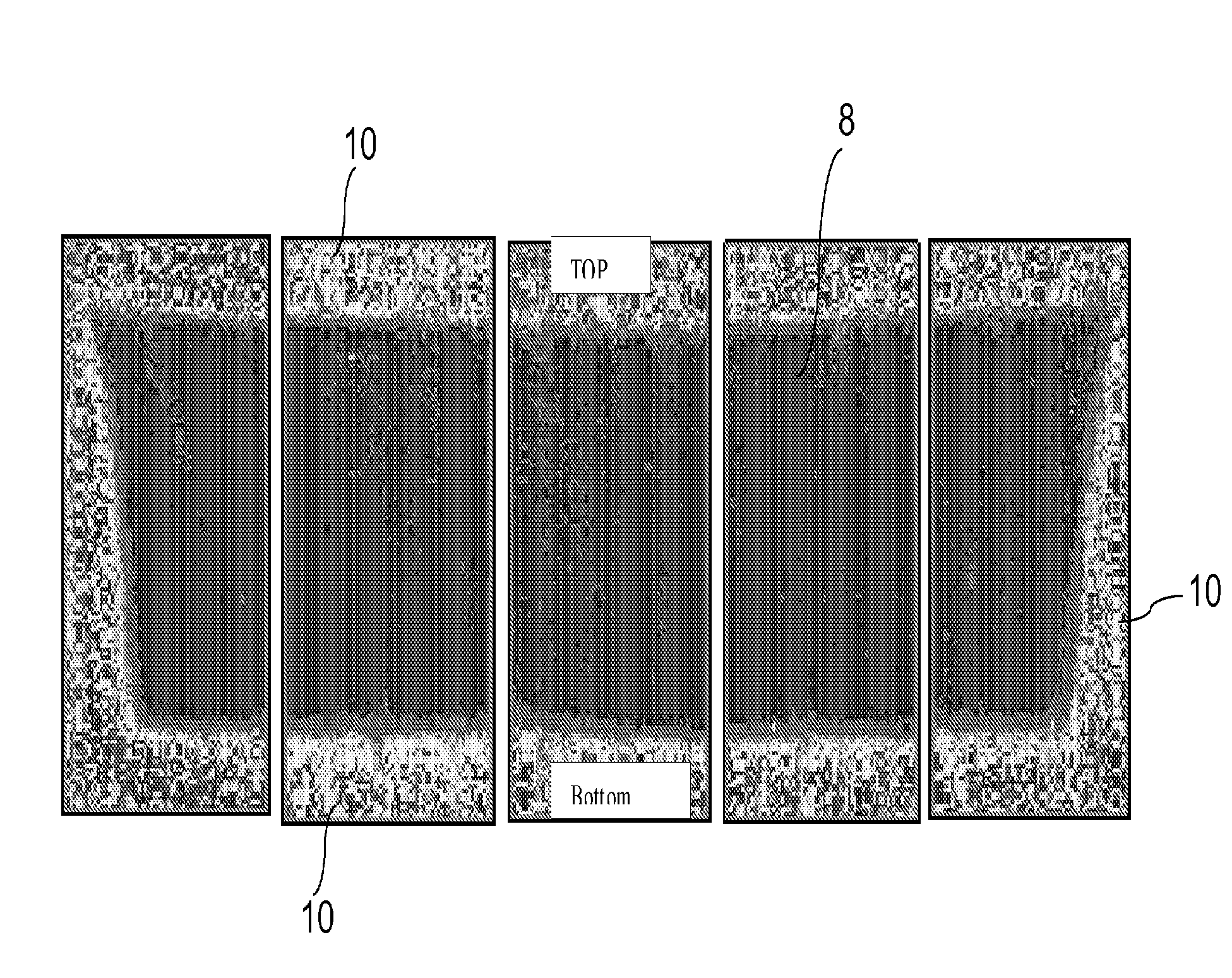
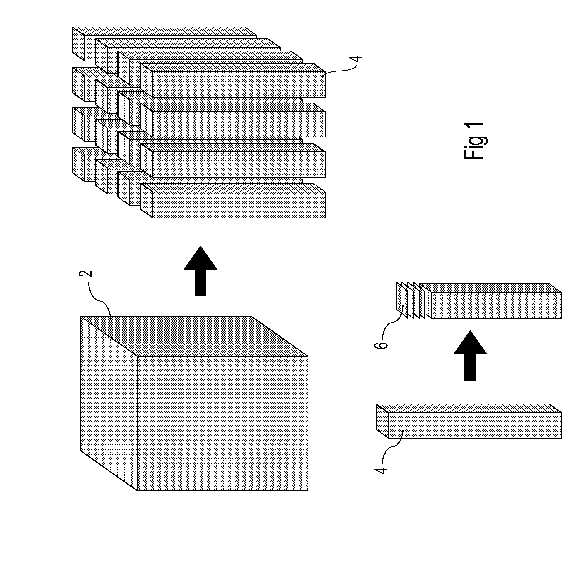
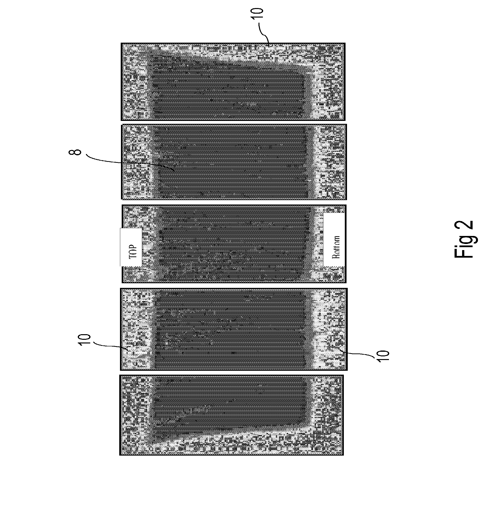
[0055]The present invention relates mainly to PL imaging measurements on ‘bulk’ silicon samples (e.g. bricks and ingots) prior to cutting into wafers. Specific advantages in relation to extracting bulk lifetime information from PL images on bricks in comparison to wafers are disclosed. The present invention details the following principal ideas, which will be described in more detail and in the same sequence below:

[0056]1.) Using information about the background doping and its spatial variation to normalise the PL image and thereby obtain more accurate quantitative information on effective or bulk lifetime variations. Specific benefits of PL imaging on bricks / ingots compared to wafer measurements for determination of bulk lifetime images, especially the ability to obtain bulk information over a much wider range of bulk lifetime values and at a well ...


PUM


Abstract

Methods are presented for separating the effects of background doping density and effective minority carrier lifetime on photoluminescence (PL) generated from semiconductor materials. In one embodiment the background doping density is measured by another technique, enabling PL measurements to be analysed in terms of effective minority carrier lifetime. In another embodiment the effective lifetime is measured by another technique, enabling PL measurements to be analysed in terms of background doping density. In yet another embodiment, the effect of background doping density is removed by calculating intensity ratios of two PL measurements obtained in different spectral regions, or generated by different excitation wavelengths. The methods are particularly useful for bulk samples such as bricks or ingots of silicon, where information can be obtained over a much wider range of bulk lifetime values than is possible with thin, surface-limited samples such as silicon wafers. The methods may find application in solar cell manufacturing for improving the manufacture of silicon ingots and bricks, or for providing a cutting guide for wafering.

Description

FIELD OF THE INVENTION[0001]The present invention relates to the characterisation of semiconductor materials using photoluminescence measurements, and in particular to techniques for separating the effects of doping density and minority carrier lifetime on the photoluminescence signal. The invention has been developed primarily for the characterisation of bulk (i.e. non-wafer) silicon samples, however it will be appreciated that the invention is not limited to this particular field of use.BACKGROUND OF THE INVENTION[0002]Commercial wafer based solar cells are made from typically 10×10 cm2 up to 22×22 cm2 silicon wafers. As illustrated in FIG. 1, a cast multicrystalline silicon block 2 (also known as an ingot), typically 1×1×0.7 m3 in size, is sawn into square (10×10 cm2 up to 22×22 cm2) shaped columns 4 (commonly known as bricks), which are then sawn into individual wafers 6, each typically 120-250 μm thick. An ingot is usually sawn into 4×4 or 5×5 bricks. Solar cells can be made fr...

Claims


Application Information

Patent Timeline
IPC IPC(8): G01N21/64
CPCH01L22/12G01N21/6489G01N2201/06113G01N2201/10
Inventor TRUPKE, THORSTEN
Owner BT IMAGING PTY LTD
Why Eureka
Try Eureka