Solar cell and its electrode structure

Inactive Publication Date: 2012-08-02
NEO SOLAR POWER CORP
View PDF8 Cites 58 Cited by
  • Summary
  • Abstract
  • Description
  • Claims
  • Application Information

AI Technical Summary

Benefits of technology

[0024]As mentioned above, in the electrode structure of the solar cell of the present invention, the bus electrodes, the finger electrodes and the connection electrode are formed by at least two screen printing processes, and at least one of the screen printing processes does not form the bus electrodes. Thus, the relative thicknesses of the finger electrodes and the bus electrodes can be controlled. In this invention, the thickness of the finger electrodes is larger than that of the bus electrodes, so th

Problems solved by technology

This is an impediment to the tr

Method used


Image

  • Solar cell and its electrode structure
  • Solar cell and its electrode structure
  • Solar cell and its electrode structure

Examples


Embodiment Construction

[0034]The present invention will be apparent from the following detailed description, which proceeds with reference to the accompanying drawings, wherein the same references relate to the same elements.

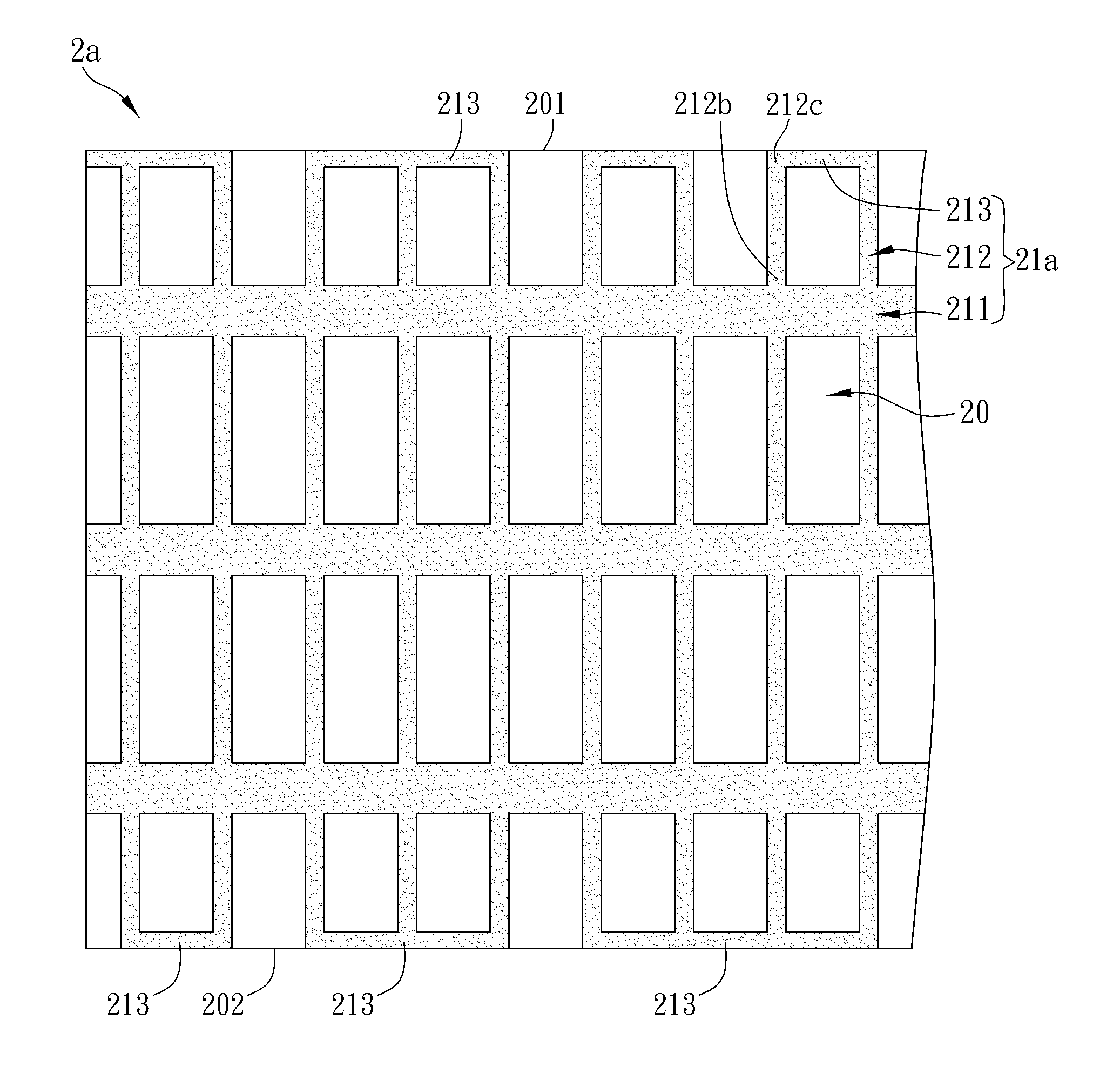
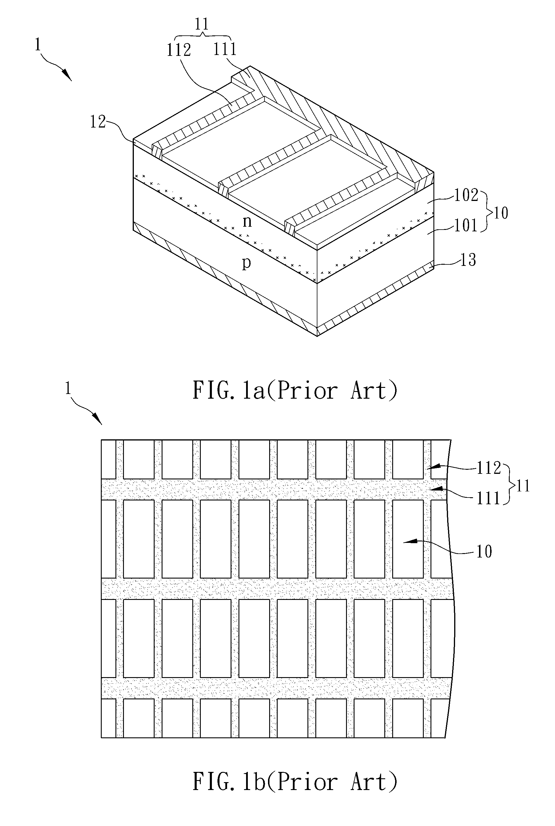
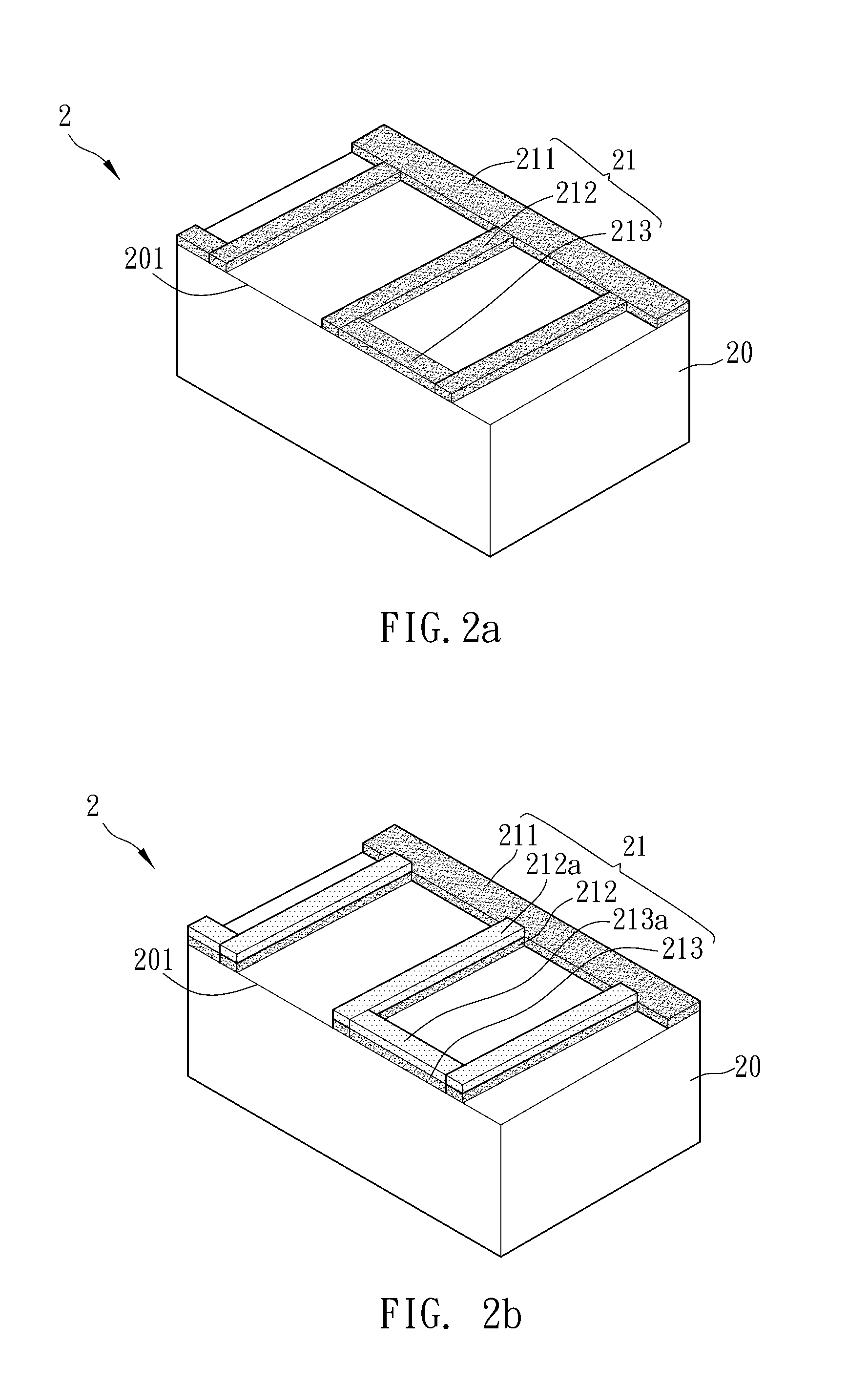
[0035]A solar cell includes a substrate and an electrode structure disposed on the substrate. The electrode structure has a plurality of layers formed by at least two screen printing processes. These layers have a first screen printed layer by a first screen printing process and a second screen printed layer by a second screen printing process. The first screen printed layer is disposed on the substrate and defines bottom portions of a plurality of finger electrodes. After the first screen printing process form the first screen printed layer, the second screen printed layer is disposed on the first screen printed layer by the second screen printing process. The second printed layer defines top portions of the finger electrodes. Both first and second printed layer define parts of the f...


PUM


Abstract

An electrode structure is disposed on a substrate of a solar cell. The electrode structure includes a plurality of bus electrodes, a plurality of finger electrodes, and at least one connection electrode. The bus electrodes are separately disposed on the substrate. The finger electrodes are disposed on two sides of the bus electrodes and electrically connect to the bus electrodes. The connection electrode is disposed on a side of the substrate and connects with at least two finger electrodes. The connection electrode, bus electrodes and the finger electrodes are formed by at least two screen printing processes, and at least one of the screen printing processes does not form the bus electrodes. Thus, the thicknesses of the finger electrodes are greater than those of the bus electrodes.

Description

CROSS REFERENCE TO RELATED APPLICATIONS[0001]This application is a Continuation-In-Part (CIP) of an earlier filed, copending U.S. Patent application, having U.S. application Ser. No. 13 / 072,655 and filed on Mar. 25, 2011, the content of which, including drawings, is expressly incorporated by reference herein.BACKGROUND OF THE INVENTION[0002]1. Field of Invention[0003]The present invention relates to an electrode structure and, in particular, to an electrode structure for a solar cell.[0004]2. Related Art[0005]The manufacture of silicon wafers is a very developed technology, and it is widely applied to the various semiconductor products. In addition, the energy gap of the silicon atoms is suitable for absorbing solar energy, so that the silicon solar cell has become the most popular solar cell. In generally, the structure of the single-crystal or poly-crystal silicon solar cell usually includes the following layers of: an external electrode, an anti-reflective layer, an N-type semico...

Claims


Application Information

Patent Timeline
IPC IPC(8): H01L31/0224
CPCH01L31/022425Y02E10/50H01L31/022433
Inventor WU, MENG-HSIUTAI, YU-WEICHEN, WEI-MINGCHEN, YANG-FANG
Owner NEO SOLAR POWER CORP
Why Eureka
Try Eureka