Check patentability & draft patents in minutes with Patsnap Eureka AI!

Photoelectric conversion element, light receiving device, light receiving system, and distance measuring device

a technology of photoelectric conversion and light receiving, which is applied in the direction of distance measurement, radiation control devices, instruments, etc., can solve the problems of time required for transferring to the output side all of the photoelectrons, the difference in the transfer efficiency between the two nodes, and the difficulty of photoelectrically converted photoelectrons to be transferred at high speeds. , to achieve the effect of improving the s/n ratio, reducing the influence of ambient light noise components, and high accuracy

Inactive Publication Date: 2012-08-02
HONDA MOTOR CO LTD
View PDF9 Cites 14 Cited by
  • Summary
  • Abstract
  • Description
  • Claims
  • Application Information

AI Technical Summary

Benefits of technology

[0009]The present invention has been made in consideration of the aforementioned problems, and has the object of providing a photoelectric conversion element in which photoelectrons obtained by photoelectric conversion can be transferred at high speeds to a desired region and accumulated therein, in which a distance measuring device can be realized by applying the principles of a TOF method, and which further enables the invention to be applied to various light receiving devices.
[0046]Still further, according to the distance measuring device of the present invention, the S / N ratio can be improved, the influence of ambient light noise components can be reduced, and the distance to an object can be measured with high accuracy.

Problems solved by technology

Accordingly, a problem occurs in that time is required for transferring to the output side all of the photoelectrons stored in the light-receiving element.
However, in the case of using a large photoelectric conversion element, the distance to the output node is long, and hence it is difficult for the photoelectrically converted photoelectrons to be transferred at high speeds to a desired node.
Furthermore, in the case that photoelectrons are allocated to two nodes from the photoelectric conversion element, if the distances to respective gate electrodes from the photoelectric conversion element are different, then a difference in the transfer efficiency to the two nodes occurs, which results in lowering of the S / N ratio, caused by the existence of an in-plane distribution in the conversion efficiency of the photoelectric conversion element, or differences in the transfer paths of the photoelectrons.

Method used


Image

  • Photoelectric conversion element, light receiving device, light receiving system, and distance measuring device
  • Photoelectric conversion element, light receiving device, light receiving system, and distance measuring device
  • Photoelectric conversion element, light receiving device, light receiving system, and distance measuring device

Examples


first embodiment

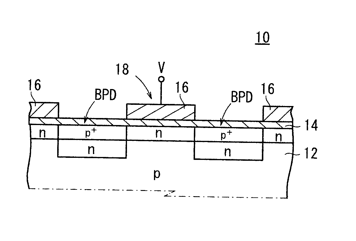
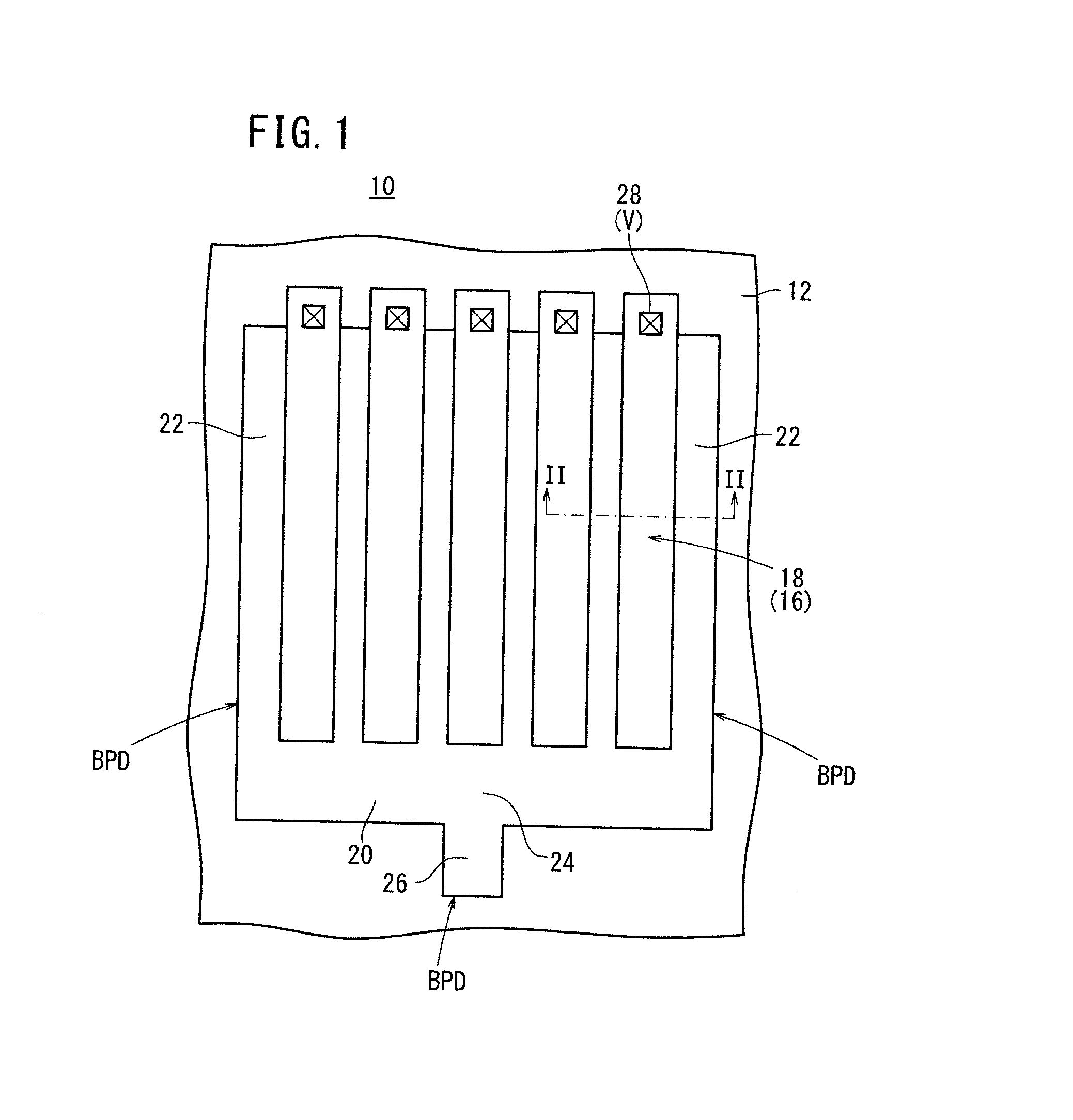
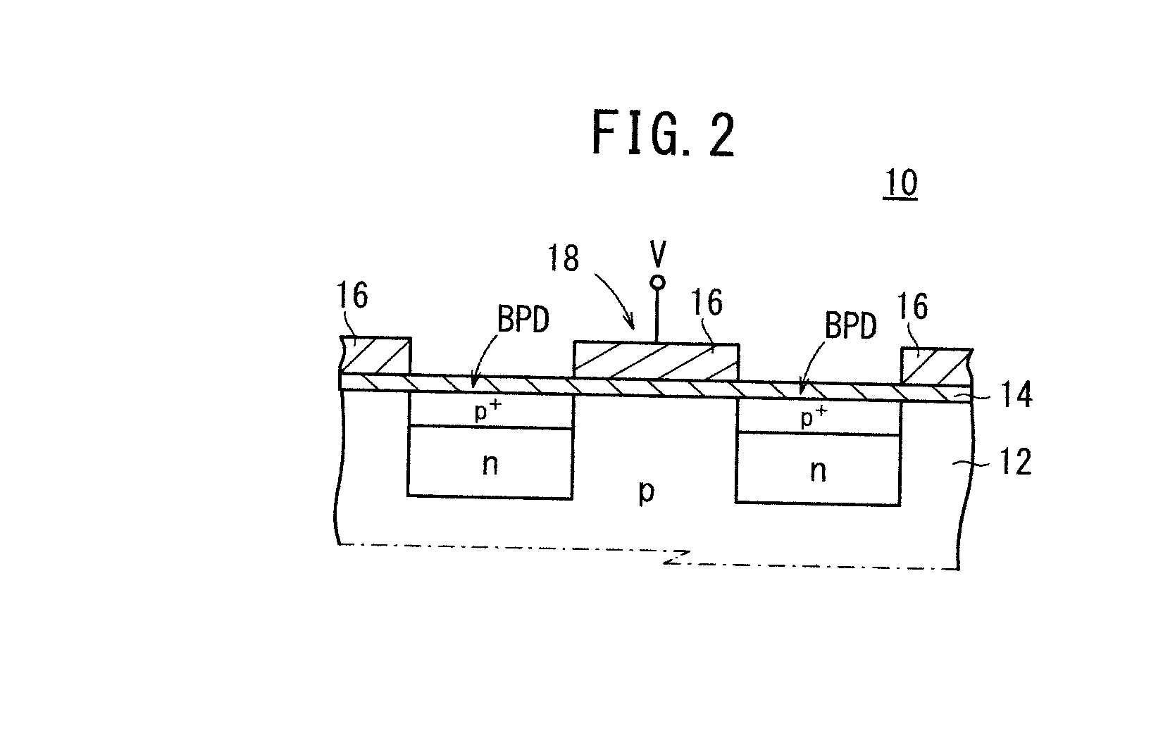
[0089]Next, a light receiving device (hereinafter referred to as a first light receiving device 100A) shall be explained with reference to FIGS. 5 and 6.

[0090]As shown in FIG. 5, the first light receiving device 100A includes a lens 102 and a first light receiving unit 104A. Incident light La that passes through the lens 102 is focused onto the first light receiving unit 104A. The lens 102 may also comprise a plurality of lenses, which are arrayed in a line or in a matrix.

[0091]As shown in FIG. 6, the first light receiving unit 104A comprises a photoelectric conversion element 10, a charge accumulating unit 26 for accumulating photoelectrons that are generated by the photoelectric conversion element 10, a capacitor Ca for storing photoelectrons at a fixed time period, a charge discharging unit 108 that discharges the photoelectrons, a first switching element SW1 disposed between the charge accumulating unit 26 and the capacitor Ca for causing the photoelectrons accumulated in the c...

second embodiment

[0102]Next, a light receiving device (hereinafter referred to as a second light receiving device 100B) shall be explained with reference to FIGS. 5 and 7.

[0103]As shown in FIG. 5, the second light receiving device 100B, similar to the aforementioned first light receiving device 100A, comprises a lens 102 and a second light receiving unit 104B.

[0104]The second light receiving unit 104B has roughly the same structure as that of the aforementioned first light receiving unit 104A of the first light receiving device 100A. However, as shown in FIG. 7, the second light receiving unit 104B differs therefrom in that a first capacitor Ca1 and a second capacitor Ca2 are included for storing photoelectrons respectively in predetermined time periods.

[0105]More specifically, the charge discharging unit 108 is arranged to confront the photoelectric conversion element 10 while sandwiching the charge accumulating unit 26 therebetween, whereas the first capacitor Ca1 and the second capacitor Ca2 are...


PUM


Abstract

A first photoelectric conversion element for detecting light and converting the light into photoelectrons comprises one buried photodiode formed in a semiconductor substrate, and a plurality of MOS diodes each having an electrode formed on the semiconductor substrate with an insulator interposed therebetween. The buried photodiode has a comb shape, in which a plurality of diverging portions are disposed to diverge from one portion, when viewed from the top thereof, and the respective electrodes of the MOS diodes are disposed so as to be nested between the plurality of diverging portions of the buried photodiode when viewed from the tops thereof.

Description

TECHNICAL FIELD[0001]The present invention relates to a photoelectric conversion element that converts light into an electric charge corresponding to the light amount thereof, a light receiving device that acquires luminance information of incident light to the photoelectric conversion element in a fixed time period, a light receiving system in which the influence of ambient light is controlled using the photoelectric conversion element, and a distance measuring device in which the principles of a time-of-flight (TOF) method are applied using the light receiving system.BACKGROUND ART[0002]Heretofore, an image sensor has been proposed, which is capable of signal detection at a high S / N ratio while removing the influence of ambient light (see, Koji Yamamoto, “Furiwake Tenso Hoshiki Oyobi Bubun Ryoiki Kosoku Yomidashi Hoshiki ni yoru Hencho Hikari Seibun Kenshutsu Kano na CMOS Image Sensor ni Kansuru Kenkyu (Research in Relation to CMOS Image Sensors Capable of Modulated Light Componen...

Claims


Application Information

Patent Timeline
Patent Type & Authority Applications(United States)
IPC IPC(8): G01C3/08H01L31/0352H01L31/0224G01S17/10G01S7/4863G01S17/894
CPCG01S7/4816G01S7/484G01S7/4868G01S7/4876G01S17/10H01L31/109H01L27/14607H01L27/1461H01L31/022408H01L31/103G01S17/89G01S7/4863G01S17/894
Inventor KAMIYAMA, TOMOYUKIKOREKADO, KEISUKE
Owner HONDA MOTOR CO LTD
Features
  • R&D
  • Intellectual Property
  • Life Sciences
  • Materials
  • Tech Scout
  • Unparalleled Data Quality
  • Higher Quality Content
  • 60% Fewer Hallucinations
Learn More