Wavelength conversion device and method of fabricating the same

a conversion device and wavelength technology, applied in the direction of optical waveguide light guide, optical element, instrument, etc., can solve the problem of small voltage in both directions, and achieve the effect of high conductive property, high transparency and improved work efficiency

Inactive Publication Date: 2012-08-02
CITIZEN FINETECH MIYOTA CO LTD +1
View PDF4 Cites 3 Cited by
  • Summary
  • Abstract
  • Description
  • Claims
  • Application Information

AI Technical Summary

Benefits of technology

[0024]The transparent electrode is formed on the surface to be bonded of the base substrate to generate the polarization inversion. The transparent electrode does not absorb the energy of the laser light even when irradiated by the laser light with the position of the wavelength conversion device and the incident position of the laser being misaligned, at the time of an inspection of a completed wavelength conversion device or an optical-axis alignment process. The optical-axis alignment process includes aligning the incident position of the laser light with the position of the completed wavelength conversion device at the subsequent assembly process. This prevents a temperature increase and peeling off of the ferroelectric single crystal substrate as in the case of using a metal electrode. Among the transparent electrodes, an ITO film and an InTiO film have high transparency and high conductive property, which leads to a preferred result. Employing the transparent electrode allows to view a surface, which is bonded to a polishing substrate, of the base substrate while grinding and polishing. Thus, an existence of air bubbles can be determined. When peeling off the base substrate from the polishing substrate after polishing, the base substrate may be peeled off while verifying a condition of delamination. This improves work efficiency. In the case where the transparent electrode is an oxide transparent electrode, an adhesive strength between the transparent electrode and the ferroelectric single crystal substrate is far more than that of a metal electrode. This also reduces delamination between the base substrate and the ferroelectric single crystal substrate at an ultrasonic cleaning after the chip processing. Further, the increased adhesive strength also improves heat resistance. Objects, characteristics, situations, and advantageous effects of the present invention will be clarified by referring to the description and the accompanying drawings below.

Problems solved by technology

This results in small voltages in both of the directions.

Method used


Image

  • Wavelength conversion device and method of fabricating the same
  • Wavelength conversion device and method of fabricating the same
  • Wavelength conversion device and method of fabricating the same

Examples


Embodiment Construction

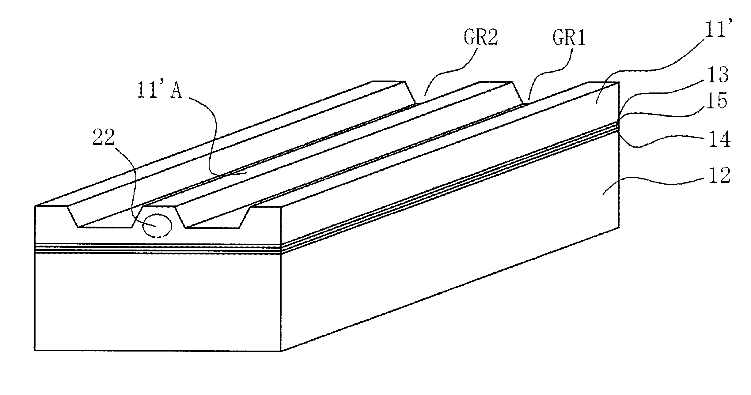
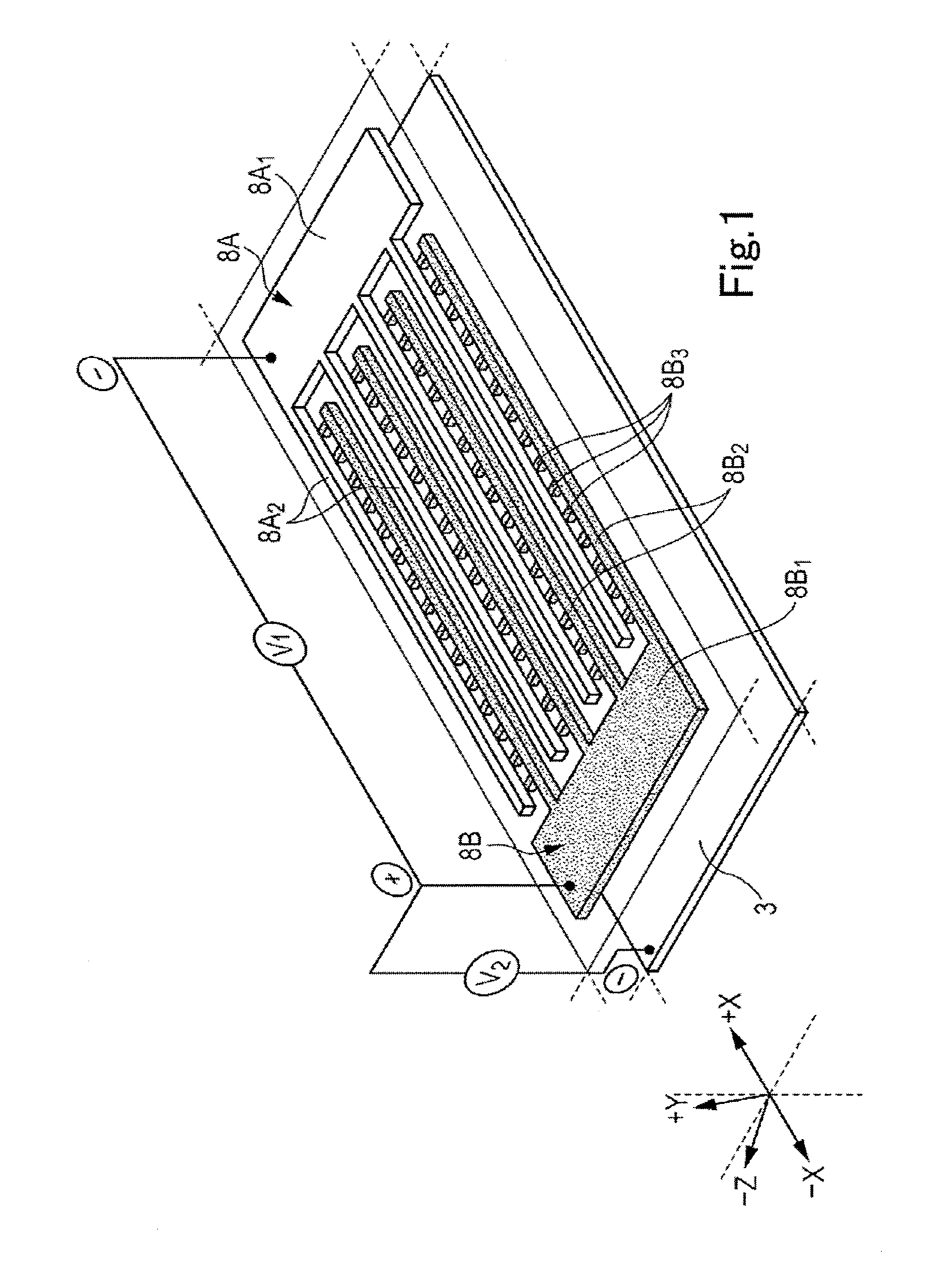
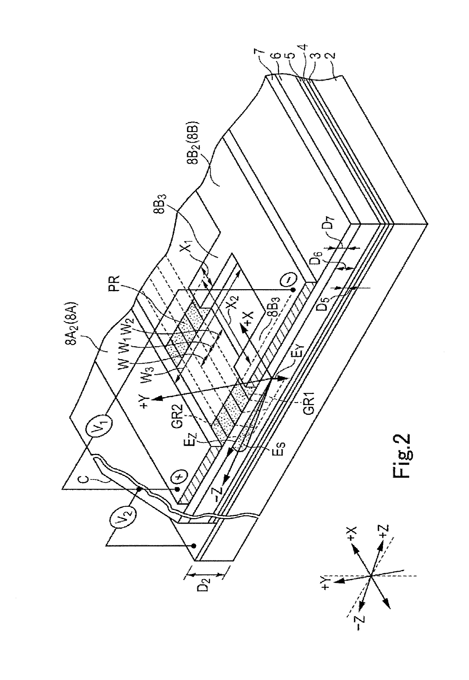
[0032]FIG. 3A to FIG. 3M are schematic block diagrams illustrating a fabricating process of the wavelength conversion device according to an embodiment of the present invention. FIG. 4A and FIG. 4B are top views of comb-shaped electrodes. FIG. 5A and FIG. 5C are schematic diagrams illustrating voltage application states at the time of the polarization inversion. FIG. 5B and FIG. 5D are respective equivalent circuit diagrams of FIG. 5A and FIG. 5C. FIG. 6 is a perspective view of the wavelength conversion devices. FIG. 7A and FIG. 7B are schematic diagrams illustrating lights entering into the wavelength conversion device.

[0033]FIG. 3A to FIG. 3M are process charts in side views illustrating a method of fabricating the wavelength conversion device according to the embodiment of the present invention. In the step illustrated in FIG. 3A, a ferroelectric single crystal substrate 11 with a thickness of 0.5 mm (for example, a 5° off y-cut substrate of MgO-doped LiNbO3) is prepared. In the...


PUM

PropertyMeasurementUnit
voltagesaaaaaaaaaa
voltagesaaaaaaaaaa
thickness D2aaaaaaaaaa

Abstract

A wavelength conversion device includes a base substrate having a transparent electrode on one surface thereof and a ferroelectric single crystal substrate provided with an optical waveguide. The ferroelectric single crystal substrate has an insulating film formed on one surface and is bonded to the base substrate such that the insulating film faces the transparent electrode.

Description

TECHNICAL FIELD[0001]The present invention relates to a wavelength conversion device and a method of fabricating the wavelength conversion device.BACKGROUND ART[0002]Use of the polarization inversion phenomenon, in which the polarization of a ferroelectric is forcibly inverted, forms a periodically poled region (a poled structure) in the ferroelectric. The poled region thus formed are employed in optical frequency modulators that use surface acoustic wave, and optical wavelength conversion devices that use polarization inversion of a nonlinear polarization. This is disclosed in Patent Document 1.[0003]FIG. 1 is a perspective view of a wavelength conversion device disclosed in Patent Document 1 (in which four devices are collectively formed). FIG. 2 is a partial enlarged perspective view of the wavelength conversion device. FIGS. 1 and 2 disclose comb-shaped electrodes 8A and 8B formed on an upper insulating layer 7. The voltage applying electrode 8A includes a rectangular-shaped mai...

Claims


Application Information

Patent Timeline
Patent Type & Authority Applications(United States)
IPC IPC(8): G02B6/12B32B38/00B32B37/14B32B37/02
CPCG02F1/3775G02F2201/124G02F2001/3548G02F1/3548
Inventor ANZAI, GAKUJIIDE, MASAFUMI
Owner CITIZEN FINETECH MIYOTA CO LTD
Why Eureka
Try Eureka