Methods For At-Speed Testing Of Memory Interface

a memory interface and at-speed testing technology, applied in the field of integrated circuit testing, can solve the problems of avoiding detection of subtle delay faults, reducing the accuracy of the output side of the memory, and reducing the accuracy of the test of the memory side, so as to reduce the power supply fluctuations, the effect of eliminating the test-dedicated circuitry

Active Publication Date: 2012-08-02
SIEMENS PROD LIFECYCLE MANAGEMENT SOFTWARE INC
View PDF7 Cites 19 Cited by
  • Summary
  • Abstract
  • Description
  • Claims
  • Application Information

AI Technical Summary

Benefits of technology

[0014]Performing the write and read operations in separate clock bursts allows for reduction of the number of at-speed clock cycles in a clock burst and thus reduction of the power supply fluctuations. Only a certain number of clock cycles in a clock burst need to be at the functional speed and the rest of the clock cycles can be slowed down.
[0015]Performing the write and read operations in separate clock bursts also enables testing of multi-port memories with asynchronous clocks. Separate read and write sequencers may be employed to ensure that the write test address is applied synchronously to the write address input of the memory and that the read test address is applied synchronously to the read address input of the memory. For memories with multiple asynchronous write ports, decode logic circuitry may be employed to prevent writing data to the same memory address from different write ports. A capture disable signal may be used and made active if the memory output is unknown. The sequence of the read operations may be modified to eliminate the need for a memory BIST circuit for small memories. If a memory has a write-all input allowing writing a data word to all memory locations in a single operation, test-dedicated circuitry may be reduced or eliminated and modified test methods may be used.

Problems solved by technology

One problem which has yet to be satisfactorily resolved is testing of a memory interface which includes a memory's test interface and surrounding functional logic that generate memory inputs and receive memory outputs.
However, the test of the output side of the memory is less accurate because the bypass flip-flops 46 update their output significantly faster than the memory 12.
As a result, subtle delay faults can escape detection by a combination of a scan test and a memory BIST test even though both tests are performed at-speed.
Another limitation is that the bypass mechanism can be relatively expensive in terms of silicon area for wide data buses.

Method used


Image

  • Methods For At-Speed Testing Of Memory Interface
  • Methods For At-Speed Testing Of Memory Interface
  • Methods For At-Speed Testing Of Memory Interface

Examples


first embodiment

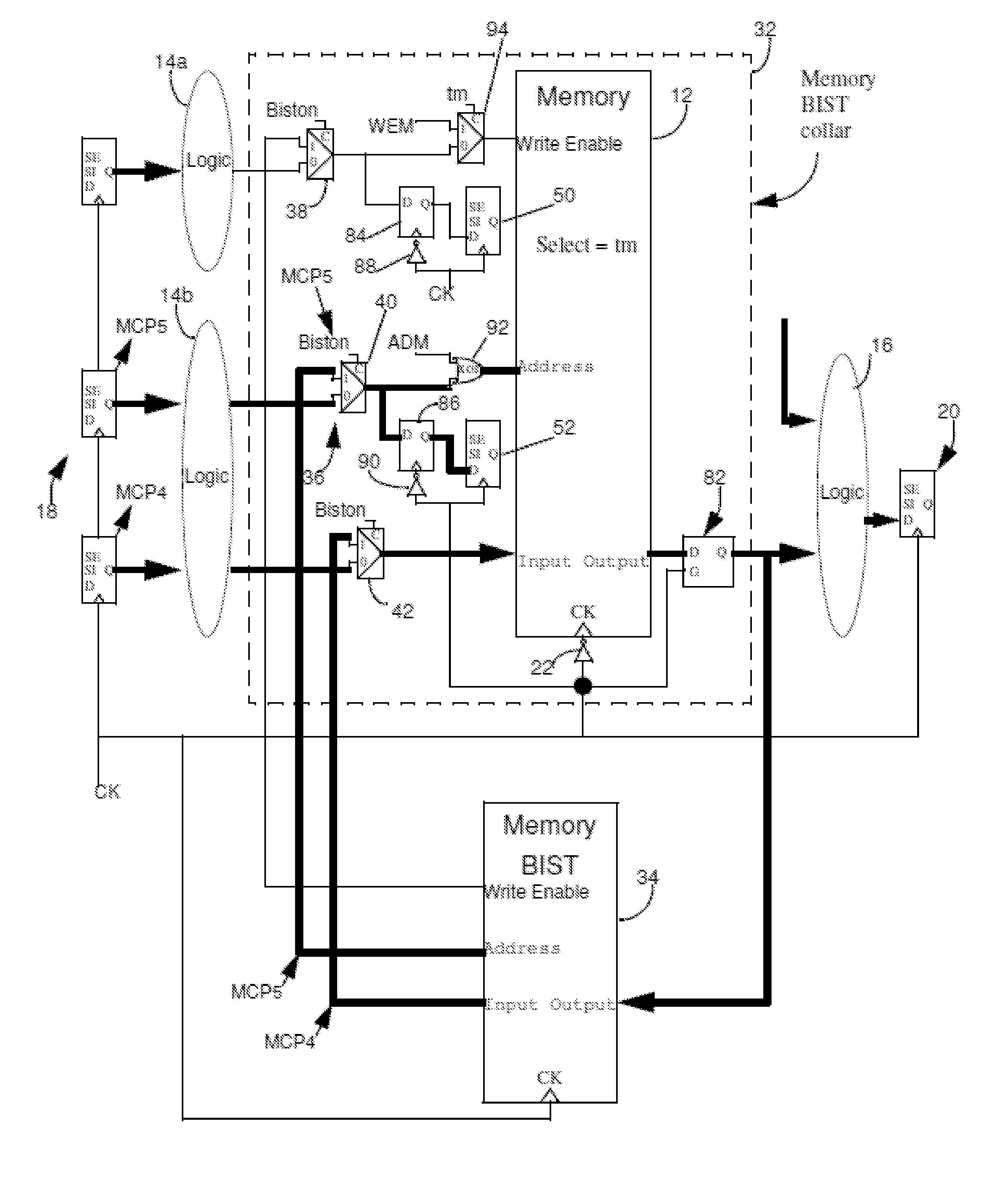
[0053]FIG. 6 illustrates a test interface for use in a circuit in which functional circuit modifications are permitted. The figure shows a circuit with an out-of-phase circuit configuration which includes an inverter 22 applied to the memory clock input and a transparent latch 82 for each memory output. The output of the transparent latches are applied to the output logic 16 and to inputs labeled “output” of memory BIST circuit 34. As in FIG. 2, each of the outputs of output logic 16 is applied to the data input of a corresponding scannable memory elements 20 of the output scan chain.

[0054]Retiming memory elements 84 and 86 are connected to the outputs of the test interface input muxes 38 and 40 associated with the write enable input and address inputs, respectively, of the memory and observation logic 50 and 52 provided for the write enable and address inputs of the memory. The clock inputs of latches 84 and 86 are inverted by inverters 88 and 90. Retiming memory elements 84 and 86...

third embodiment

[0070]Advantageously, these embodiments of the invention typically do not require functional changes to the memory circuit. This has several implications. First, there is no need to reduce at-speed coverage of other destinations. Second, it is applicable to more circuits (e.g., where the data and / or address is provided by another memory). Third, there is no introduction of asynchronous loops or redundant faults. Fourth, it has reduced combinational depth; the memory output is directly controllable from a set of dedicated registers and limit the combinational depth of the circuit as compared to the embodiment of FIG. 6 and there are no combinational paths that traverse the memory. Fifth, there is no need to modify the BIST controller itself except for the address counter in the illustrated examples. This requirement can be relaxed by using the address observation flip-flops to provide the address. This is discussed in more detail in the description of the third embodiment below. Sixt...


PUM


Abstract

Methods for at-speed testing of a memory interface associated with an embedded memory involves in general two write operations in succession, two read operations in succession, and a capture operation using scan cells. The write and read operations may be performed during a single clock burst, two separate clock bursts in a clock signal, or two separate clock bursts in separate clock signals.

Description

RELATED APPLICATIONS[0001]This application claims priority under 35 U.S.C. §120 to U.S. patent application Ser. No. 12 / 579,572, filed on Oct. 15, 2009, and naming Benoit Nadeau-Dostie et al. as inventors, which application in turn claims priority under 35 U.S.C. §120 of U.S. patent application Ser. No. 11 / 439,497, filed on May 24, 2006, naming Benoit Nadeau-Dostie et al. as inventors (now U.S. Pat. No. 7,617,425), which in turn claimed priority under 35 U.S.C. §119 to U.S. Provisional Patent Application No. 60 / 693,778, filed on Jun. 27, 2005, and naming Benoit Nadeau-Dostie et al. as inventors. Each of these applications is incorporated entirely herein by reference.FIELD OF THE INVENTION[0002]The present invention is directed to the testing of integrated circuits. Various aspects of the invention may be particularly useful for at-speed testing of memory interfaces.BACKGROUND OF THE INVENTION[0003]The main challenges facing semiconductor manufacturers and integrated circuit designers...

Claims


Application Information

Patent Timeline
Patent Type & Authority Applications(United States)
IPC IPC(8): G11C29/10G06F11/263
CPCG11C8/16G11C29/50012G11C29/32G11C29/1201
Inventor NADEAU-DOSTIE, BENOITCOTE, JEAN-FRANCOIS
Owner SIEMENS PROD LIFECYCLE MANAGEMENT SOFTWARE INC
Why Eureka
Try Eureka